目录VUj嘉泰姆
1.产品概述 2.产品特点
3.应用范围 4.下载产品资料PDF文档
5.产品封装图</span> 6.电路原理图</span>
7.功能概述 8.相关产品VUj嘉泰姆
一,产品概述(General Description) VUj嘉泰姆
The CXSD62115, two-phase PWM control IC, provides a precision voltage regulation system for advanced graphic microprocessors in graphics card applications. The inte-gration of power MOSFET drivers into the controller IC
reduces the number of external parts for a cost and space saving power management solution.
The CXSD62115 uses a voltage-mode PWM architecture,operating with fixed-frequency, to provide excellent load transient response. The device uses the voltage across the DCRs of the inductors for current sensing. Load line
voltage positioning (DROOP), channel-current balance,and over-current protection are accomplished through continuous inductor DCR current sensing.
The MODE pin programs single- or two- phase operation.When IC operates in two-phase mode normally, it can transfer two-phase mode to single phase mode at liberty.Nevertheless, once operates in single-phase mode, the operation mode is latched. It is required to toggle SS or 5VCC pin to reset the IC. Such feature of the MODE pin makes the CXSD62115 ideally suitable for dual power input applications, such as PCIE interfaced graphic cards. This control IC‘s protection features include a set of so- phisticated over-temperature, over-voltage, under-voltage, and over-current protections. Over-voltage results in the converter turning the lower MOSFETs on to clamp the rising output voltage and protects the microprocessor.The over-current protection level is set through externalresistors. The device also provides a power-on-reset func-tion and a programmable soft-start to prevent wrong op-eration and limit the input surge current during power-on or start-up.
The CXSD62115 is available in a QFN4x4-24A package
二</span>.产品特点(Features)VUj嘉泰姆
Voltage-Mode Operation with Current Sharing
- Adjustable Feedback Compensation
- Fast Load Transient Response
Operate with 8V~13.2 VCC Supply Voltage
Programmable 3-Bit DAC Reference
-±1.5% System Accuracy Over-Temperature
Support Single- and Two-Phase Operations
5V Linear Regulator Output on 5VCC
8~12V Gate Drivers with Internal Bootstrap Diode
Lossless Inductor DCR Current Sensing
Fixed 300kHz Operating Frequency Per Phase
Power-OK Indicator Output
- Regulated 1.5V on POK
Adjustable Over-Current Protection (OCP)
Accurate Load Line (DROOP) Programming
Adjustable Soft-Start
Over-Voltage Protection (OVP)
Under-Voltage Protection (UVP)
Over-Temperature Protection (OTP)
QFN4x4 24-Lead Package (QFN4x4-24A)
Lead Free and Green Devices Available
(RoHS Compliant)
三</span>,应用范围 (Applications)VUj嘉泰姆
Graphics Card GPU Core Power SupplyVUj嘉泰姆
Motherboard Chipset or DDR SDRAM Core Power Supply
On-Board High Power PWM Converter withVUj嘉泰姆
Output Current up to 60A
四.下载产品资料PDF文档 VUj嘉泰姆
需要详细的PDF规格书请扫一扫微信联系我们,还可以获得免费样品以及技术支持</span>!</span>VUj嘉泰姆
 VUj嘉泰姆
五,产品封装图 (Package)VUj嘉泰姆
 VUj嘉泰姆
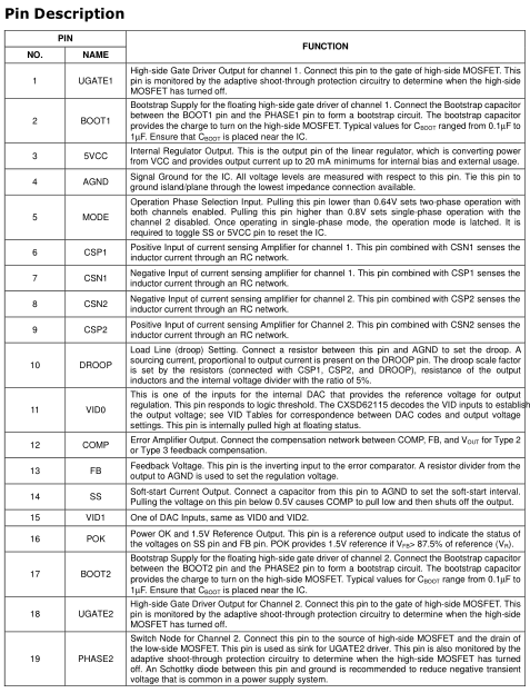
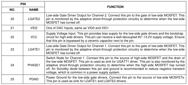 VUj嘉泰姆
六.电路原理图</span>VUj嘉泰姆
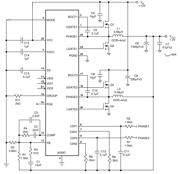 VUj嘉泰姆
七</span>,功能概述VUj嘉泰姆
Layout Consideration VUj嘉泰姆
In any high switching frequency converter, a correct lay-out is important to ensure proper operation of the
regulator. With power devices switching at higher frequency, the resulting current transient will cause volt-
age spike across the interconnecting impedance and parasitic circuit elements. As an example, consider the
turn-off transition of the PWM MOSFET. Before turn-off condition, the MOSFET is carrying the full load current.
During turn-off, current stops flowing in the MOSFET and is freewheeling by the lower MOSFET and parasitic diode.
Any parasitic inductance of the circuit generates a large voltage spike during the switching interval. In general,
using short and wide printed circuit traces should mini-mize interconnecting impedances and the magnitude of
voltage spike. And signal and power grounds are to be kept separating and finally combined to use the ground
plane construction or single point grounding. The best tie-point between the signal ground and the power ground is at the negative side of the output capacitor on each channel, where there is less noise. Noisy traces beneath the IC are not recommended. Below is a checklist for your layout:
close their pins. (For example, place the decoupling ce-ramic capacitor near the drain of the high-side MOSFET
as close as possible. The bulk capacitors are also placed near the drain).
- The input capacitor should be near the drain of the up-per MOSFET; the high quality ceramic decoupling capaci-tor can be put close to the VCC and GND pins; the VTTREF decoupling capacitor should be close to the VTTREF pin and GND; the VDDQ and VTT output capacitors should be located right across their output pin as close as pos-sible to the part to minimize parasitic. The input capacitor GND should be close to the output capacitor GND and the lower MOSFET GND.
- The drain of the MOSFETs (VIN and PHASE nodes) should be a large plane for heat sinking. And PHASE pin
traces are also the return path for UGATE. Connect this pin to the converter’s upper MOSFET source.
- The CXSD62115 used ripple mode control. Build the re- sistor divider close to the VFB pin so that the high imped- ance trace is shorter. And the VFB pin traces can’t be closed to the switching signal traces (UGATE, LGATE,BOOT, and PHASE).
- The PGND trace should be a separate trace, and inde-pendently go to the source of the low-side MOSFETs for
current limit accuracy.VUj嘉泰姆
Layout Consideration
- Keep the switching nodes (UGATE, LGATE, BOOT, and PHASE) away from sensitive small signal nodes(VFB,VTTREF, and CS) since these nodes are fast moving signals. Therefore, keep traces to these nodes as short as possible and there should be no other weak signal traces in parallel with theses traces on any layer.
- The signals going through theses traces have both high dv/dt and high di/dt, with high peak charging and dis-charging current. The traces from the gate drivers to the MOSFETs (UGATE and LGATE) should be short and wide.
- Place the source of the high-side MOSFET and the drain of the low-side MOSFET as close as possible. Minimiz-ing the impedance with wide layout plane between the two pads reduces the voltage bounce of the node.VUj嘉泰姆
- Decoupling VUj嘉泰姆
capacitor, the resistor dividers, boot capacitors, and current limit stetting resistor should beVUj嘉泰姆
CXSD62115VUj嘉泰姆
八,相关产品 更多同类产品...... VUj嘉泰姆
Switching Regulator > Buck ControllerVUj嘉泰姆 |
Part_No VUj嘉泰姆 | Package VUj嘉泰姆 | ArchiVUj嘉泰姆 tectuVUj嘉泰姆 | PhaseVUj嘉泰姆 | No.ofVUj嘉泰姆 PWMVUj嘉泰姆 OutputVUj嘉泰姆 | Output VUj嘉泰姆 CurrentVUj嘉泰姆 (A) VUj嘉泰姆 | InputVUj嘉泰姆 Voltage (V) VUj嘉泰姆 | ReferenceVUj嘉泰姆 VoltageVUj嘉泰姆 (V) VUj嘉泰姆 | Bias VUj嘉泰姆 VoltageVUj嘉泰姆 (V) VUj嘉泰姆 | QuiescentVUj嘉泰姆 CurrentVUj嘉泰姆 (uA) VUj嘉泰姆 |
minVUj嘉泰姆 | maxVUj嘉泰姆 |
CXSD6273VUj嘉泰姆 | SOP-14VUj嘉泰姆 QSOP-16VUj嘉泰姆 QFN4x4-16VUj嘉泰姆 | VM VUj嘉泰姆 | 1 VUj嘉泰姆 | 1 VUj嘉泰姆 | 30VUj嘉泰姆 | 2.9 VUj嘉泰姆 | 13.2VUj嘉泰姆 | 0.9VUj嘉泰姆 | 12 VUj嘉泰姆 | 8000VUj嘉泰姆 |
CXSD6274VUj嘉泰姆 | SOP-8VUj嘉泰姆 | VM VUj嘉泰姆 | 1VUj嘉泰姆 | 1VUj嘉泰姆 | 20VUj嘉泰姆 | 2.9 VUj嘉泰姆 | 13.2 VUj嘉泰姆 | 0.8VUj嘉泰姆 | 12VUj嘉泰姆 | 5000VUj嘉泰姆 |
CXSD6274CVUj嘉泰姆 | SOP-8VUj嘉泰姆 | VMVUj嘉泰姆 | 1VUj嘉泰姆 | 1VUj嘉泰姆 | 20VUj嘉泰姆 | 2.9VUj嘉泰姆 | 13.2VUj嘉泰姆 | 0.8VUj嘉泰姆 | 12VUj嘉泰姆 | 5000VUj嘉泰姆 |
CXSD6275VUj嘉泰姆 | QFN4x4-24VUj嘉泰姆 | VMVUj嘉泰姆 | 2VUj嘉泰姆 | 1VUj嘉泰姆 | 60VUj嘉泰姆 | 3.1VUj嘉泰姆 | 13.2VUj嘉泰姆 | 0.6VUj嘉泰姆 | 12VUj嘉泰姆 | 5000VUj嘉泰姆 |
CXSD6276VUj嘉泰姆 | SOP-8VUj嘉泰姆 | VMVUj嘉泰姆 | 1VUj嘉泰姆 | 1VUj嘉泰姆 | 20VUj嘉泰姆 | 2.2VUj嘉泰姆 | 13.2VUj嘉泰姆 | 0.8VUj嘉泰姆 | 5~12VUj嘉泰姆 | 2100VUj嘉泰姆 |
CXSD6276AVUj嘉泰姆 | SOP-8VUj嘉泰姆 | VMVUj嘉泰姆 | 1VUj嘉泰姆 | 1VUj嘉泰姆 | 20VUj嘉泰姆 | 2.2VUj嘉泰姆 | 13.2VUj嘉泰姆 | 0.8VUj嘉泰姆 | 5~12VUj嘉泰姆 | 2100VUj嘉泰姆 |
CXSD6277/A/BVUj嘉泰姆 | SOP8|TSSOP8VUj嘉泰姆 | VMVUj嘉泰姆 | 1VUj嘉泰姆 | 1VUj嘉泰姆 | 5VUj嘉泰姆 | 5VUj嘉泰姆 | 13.2VUj嘉泰姆 | 1.25|0.8VUj嘉泰姆 | 5~12VUj嘉泰姆 | 3000VUj嘉泰姆 |
CXSD6278VUj嘉泰姆 | SOP-8VUj嘉泰姆 | VMVUj嘉泰姆 | 1VUj嘉泰姆 | 1VUj嘉泰姆 | 10VUj嘉泰姆 | 3.3VUj嘉泰姆 | 5.5VUj嘉泰姆 | 0.8VUj嘉泰姆 | 5VUj嘉泰姆 | 2100VUj嘉泰姆 |
CXSD6279BVUj嘉泰姆 | SOP-14VUj嘉泰姆 | VM VUj嘉泰姆 | 1VUj嘉泰姆 | 1VUj嘉泰姆 | 10VUj嘉泰姆 | 5VUj嘉泰姆 | 13.2VUj嘉泰姆 | 0.8VUj嘉泰姆 | 12VUj嘉泰姆 | 2000VUj嘉泰姆 |
CXSD6280VUj嘉泰姆 | TSSOP-24VUj嘉泰姆 |QFN5x5-32VUj嘉泰姆 | VMVUj嘉泰姆 | 1VUj嘉泰姆 | 2VUj嘉泰姆 | 20VUj嘉泰姆 | 5VUj嘉泰姆 | 13.2VUj嘉泰姆 | 0.6VUj嘉泰姆 | 5~12VUj嘉泰姆 | 4000VUj嘉泰姆 |
CXSD6281NVUj嘉泰姆 | SOP14VUj嘉泰姆 QSOP16VUj嘉泰姆 QFN-16VUj嘉泰姆 | VMVUj嘉泰姆 | 1VUj嘉泰姆 | 1VUj嘉泰姆 | 30VUj嘉泰姆 | 2.9VUj嘉泰姆 | 13.2VUj嘉泰姆 | 0.9VUj嘉泰姆 | 12VUj嘉泰姆 | 4000VUj嘉泰姆 |
CXSD6282VUj嘉泰姆 | SOP-14VUj嘉泰姆 | VMVUj嘉泰姆 | 1VUj嘉泰姆 | 1VUj嘉泰姆 | 30VUj嘉泰姆 | 2.2VUj嘉泰姆 | 13.2VUj嘉泰姆 | 0.6VUj嘉泰姆 | 12VUj嘉泰姆 | 5000VUj嘉泰姆 |
CXSD6282AVUj嘉泰姆 | SOP-14VUj嘉泰姆 | VMVUj嘉泰姆 | 1VUj嘉泰姆 | 1VUj嘉泰姆 | 30VUj嘉泰姆 | 2.2VUj嘉泰姆 | 13.2VUj嘉泰姆 | 0.6VUj嘉泰姆 | 12VUj嘉泰姆 | 5000VUj嘉泰姆 |
CXSD6283VUj嘉泰姆 | SOP-14VUj嘉泰姆 | VMVUj嘉泰姆 | 1VUj嘉泰姆 | 1VUj嘉泰姆 | 25VUj嘉泰姆 | 2.2VUj嘉泰姆 | 13.2VUj嘉泰姆 | 0.8VUj嘉泰姆 | 12VUj嘉泰姆 | 5000VUj嘉泰姆 |
CXSD6284/AVUj嘉泰姆 | LQFP7x7 48VUj嘉泰姆 TQFN7x7-48VUj嘉泰姆 | VMVUj嘉泰姆 | 1VUj嘉泰姆 | 6VUj嘉泰姆 | 0.015VUj嘉泰姆 | 1.4VUj嘉泰姆 | 6.5VUj嘉泰姆 | -VUj嘉泰姆 | 5VUj嘉泰姆 | 1800VUj嘉泰姆 |
CXSD6285VUj嘉泰姆 | TSSOP-24PVUj嘉泰姆 | VMVUj嘉泰姆 | 1VUj嘉泰姆 | 2VUj嘉泰姆 | 20VUj嘉泰姆 | 2.97VUj嘉泰姆 | 5.5VUj嘉泰姆 | 0.8VUj嘉泰姆 | 5~12VUj嘉泰姆 | 5000VUj嘉泰姆 |
CXSD6286VUj嘉泰姆 | SOP-14VUj嘉泰姆 | VMVUj嘉泰姆 | 1VUj嘉泰姆 | 1VUj嘉泰姆 | 10VUj嘉泰姆 | 5VUj嘉泰姆 | 13.2VUj嘉泰姆 | 0.8VUj嘉泰姆 | 12VUj嘉泰姆 | 3000VUj嘉泰姆 |
CXSD6287VUj嘉泰姆 | SOP-8-P|DIP-8VUj嘉泰姆 | VMVUj嘉泰姆 | 1VUj嘉泰姆 | 1VUj嘉泰姆 | 30VUj嘉泰姆 | 2.9VUj嘉泰姆 | 13.2VUj嘉泰姆 | 1.2VUj嘉泰姆 | 12VUj嘉泰姆 | 3000VUj嘉泰姆 |
CXSD6288VUj嘉泰姆 | SSOP28VUj嘉泰姆 QFN4x4-24VUj嘉泰姆 | VMVUj嘉泰姆 | 1VUj嘉泰姆 | 2VUj嘉泰姆 | 20VUj嘉泰姆 | 5VUj嘉泰姆 | 24VUj嘉泰姆 | 0.9VUj嘉泰姆 | 5VUj嘉泰姆 | 1200VUj嘉泰姆 |
CXSD6289VUj嘉泰姆 | SOP-20VUj嘉泰姆 | VMVUj嘉泰姆 | 1VUj嘉泰姆 | 2VUj嘉泰姆 | 20VUj嘉泰姆 | 2.2VUj嘉泰姆 | 13.2VUj嘉泰姆 | 0.6VUj嘉泰姆 | 5~12VUj嘉泰姆 | 4000VUj嘉泰姆 |
CXSD6290VUj嘉泰姆 | SOP8|DFN3x3-10VUj嘉泰姆 | VMVUj嘉泰姆 | 1VUj嘉泰姆 | 2VUj嘉泰姆 | -VUj嘉泰姆 | -VUj嘉泰姆 | -VUj嘉泰姆 | -VUj嘉泰姆 | 5~12VUj嘉泰姆 | 550VUj嘉泰姆 |
CXSD6291HCVUj嘉泰姆 | DIP8|SOP-8VUj嘉泰姆 | VMVUj嘉泰姆 | 1VUj嘉泰姆 | 1VUj嘉泰姆 | 1VUj嘉泰姆 | 1.2VUj嘉泰姆 | 9VUj嘉泰姆 | 24VUj嘉泰姆 | 5VUj嘉泰姆 | 9 ~ 24VUj嘉泰姆 |
CXSD6292VUj嘉泰姆 | SSOP16VUj嘉泰姆 QFN4x4-16VUj嘉泰姆 TQFN3x3-16VUj嘉泰姆 | VMVUj嘉泰姆 | 1VUj嘉泰姆 | 1VUj嘉泰姆 | 25VUj嘉泰姆 | 3VUj嘉泰姆 | 25VUj嘉泰姆 | 0.6VUj嘉泰姆 | 5VUj嘉泰姆 | 1700VUj嘉泰姆 |
CXSD6293VUj嘉泰姆 | TDFN3x3-10VUj嘉泰姆 | COTVUj嘉泰姆 | 1VUj嘉泰姆 | 1VUj嘉泰姆 | 25VUj嘉泰姆 | 3VUj嘉泰姆 | 25VUj嘉泰姆 | 0.5VUj嘉泰姆 | 5VUj嘉泰姆 | 350VUj嘉泰姆 |
CXSD6294VUj嘉泰姆 | QFN4x4-24VUj嘉泰姆 | CMVUj嘉泰姆 | 2VUj嘉泰姆 | 1VUj嘉泰姆 | 40VUj嘉泰姆 | 4.5VUj嘉泰姆 | 13.2VUj嘉泰姆 | 0.6VUj嘉泰姆 | 5~12VUj嘉泰姆 | 4000VUj嘉泰姆 |
CXSD6295VUj嘉泰姆 | SOP8PVUj嘉泰姆 TDFN3x3-10VUj嘉泰姆 | VMVUj嘉泰姆 | 1VUj嘉泰姆 | 1VUj嘉泰姆 | 20VUj嘉泰姆 | 3VUj嘉泰姆 | 13.2VUj嘉泰姆 | 0.8VUj嘉泰姆 | 5~12VUj嘉泰姆 | 2500VUj嘉泰姆 |
CXSD6296A|B|C|DVUj嘉泰姆 | SOP8PVUj嘉泰姆 | VMVUj嘉泰姆 | 1VUj嘉泰姆 | 1VUj嘉泰姆 | 25VUj嘉泰姆 | 3VUj嘉泰姆 | 13.2VUj嘉泰姆 | 0.6|0.8VUj嘉泰姆 | 5~12VUj嘉泰姆 | 1200VUj嘉泰姆 |
CXSD6297VUj嘉泰姆 | TDFN3x3-10VUj嘉泰姆 | VMVUj嘉泰姆 | 1VUj嘉泰姆 | 1VUj嘉泰姆 | 25VUj嘉泰姆 | 4VUj嘉泰姆 | 13.2VUj嘉泰姆 | 0.8VUj嘉泰姆 | 5~12VUj嘉泰姆 | 2000VUj嘉泰姆 |
CXSD6298VUj嘉泰姆 | TDFN3x3-10VUj嘉泰姆 | COTVUj嘉泰姆 | 1VUj嘉泰姆 | 1VUj嘉泰姆 | 25VUj嘉泰姆 | 4.5VUj嘉泰姆 | 25VUj嘉泰姆 | 0.6VUj嘉泰姆 | 5~12VUj嘉泰姆 | 80VUj嘉泰姆 |
CXSD6299|AVUj嘉泰姆 | SOP-8PVUj嘉泰姆 | VMVUj嘉泰姆 | 1VUj嘉泰姆 | 1VUj嘉泰姆 | 25VUj嘉泰姆 | 4.5VUj嘉泰姆 | 13.2VUj嘉泰姆 | 0.8VUj嘉泰姆 | 5~12VUj嘉泰姆 | 16000VUj嘉泰姆 |
CXSD62100VUj嘉泰姆 | TQFN3x3-10VUj嘉泰姆 | VMVUj嘉泰姆 | 1VUj嘉泰姆 | 1VUj嘉泰姆 | 25VUj嘉泰姆 | 4.5VUj嘉泰姆 | 13.2VUj嘉泰姆 | 0.6VUj嘉泰姆 | 5~12VUj嘉泰姆 | 2500VUj嘉泰姆 |
CXSD62101|LVUj嘉泰姆 | TDFN3x3-10VUj嘉泰姆 | COTVUj嘉泰姆 | 1VUj嘉泰姆 | 1VUj嘉泰姆 | 30VUj嘉泰姆 | 3VUj嘉泰姆 | 25VUj嘉泰姆 | 0.8VUj嘉泰姆 | 5~12VUj嘉泰姆 | 2000VUj嘉泰姆 |
CXSD62102VUj嘉泰姆 | TQFN3x3-16VUj嘉泰姆 | COTVUj嘉泰姆 | 1VUj嘉泰姆 | 1VUj嘉泰姆 | 30VUj嘉泰姆 | 1.8VUj嘉泰姆 | 28VUj嘉泰姆 | 0.6VUj嘉泰姆 | 5VUj嘉泰姆 | 600VUj嘉泰姆 |
CXSD62102AVUj嘉泰姆 | TQFN 3x3 16VUj嘉泰姆 | COTVUj嘉泰姆 | 1VUj嘉泰姆 | 1VUj嘉泰姆 | 30VUj嘉泰姆 | 1.8VUj嘉泰姆 | 28VUj嘉泰姆 | 0.6VUj嘉泰姆 | 5VUj嘉泰姆 | 600VUj嘉泰姆 |
CXSD62103VUj嘉泰姆 | QFN4x4-24VUj嘉泰姆 | VMVUj嘉泰姆 | 2VUj嘉泰姆 | 1VUj嘉泰姆 | 50VUj嘉泰姆 | 4.5VUj嘉泰姆 | 13.2VUj嘉泰姆 | 0.6VUj嘉泰姆 | 5~12VUj嘉泰姆 | 5000VUj嘉泰姆 |
CXSD62104VUj嘉泰姆 | TQFN4x4-24VUj嘉泰姆 | COTVUj嘉泰姆 | 1VUj嘉泰姆 | 2VUj嘉泰姆 | 15VUj嘉泰姆 | 6VUj嘉泰姆 | 25VUj嘉泰姆 | 2VUj嘉泰姆 | NVUj嘉泰姆 | 550VUj嘉泰姆 |
CXSD62105VUj嘉泰姆 | TQFN4x4-24VUj嘉泰姆 | COTVUj嘉泰姆 | 1VUj嘉泰姆 | 2VUj嘉泰姆 | 15VUj嘉泰姆 | 6VUj嘉泰姆 | 25VUj嘉泰姆 | 2VUj嘉泰姆 | NVUj嘉泰姆 | 550VUj嘉泰姆 |
CXSD62106|AVUj嘉泰姆 | TQFN4x4-4VUj嘉泰姆 TQFN3x3-20VUj嘉泰姆 | COTVUj嘉泰姆 | 1VUj嘉泰姆 | 2VUj嘉泰姆 | 20VUj嘉泰姆 | 3VUj嘉泰姆 | 28VUj嘉泰姆 | 0.75VUj嘉泰姆 | 5VUj嘉泰姆 | 800VUj嘉泰姆 |
CXSD62107VUj嘉泰姆 | TQFN3x3-16VUj嘉泰姆 | COTVUj嘉泰姆 | 1VUj嘉泰姆 | 1VUj嘉泰姆 | 20VUj嘉泰姆 | 1.8VUj嘉泰姆 | 28VUj嘉泰姆 | 0.75VUj嘉泰姆 | 5VUj嘉泰姆 | 400VUj嘉泰姆 |
CXSD62108VUj嘉泰姆 | QFN3.5x3.5-14VUj嘉泰姆 TQFN3x3-16VUj嘉泰姆 | COTVUj嘉泰姆 | 1VUj嘉泰姆 | 1VUj嘉泰姆 | 20VUj嘉泰姆 | 1.8VUj嘉泰姆 | 28VUj嘉泰姆 | 0.75VUj嘉泰姆 | 5VUj嘉泰姆 | 400VUj嘉泰姆 |
CXSD62109VUj嘉泰姆 | TQFN3x3-16VUj嘉泰姆 | COTVUj嘉泰姆 | 1VUj嘉泰姆 | 2VUj嘉泰姆 | 20VUj嘉泰姆 | 1.8VUj嘉泰姆 | 28VUj嘉泰姆 | 0.75VUj嘉泰姆 | 5VUj嘉泰姆 | 400VUj嘉泰姆 |
CXSD62110VUj嘉泰姆 | QFN3x3-20VUj嘉泰姆 TQFN3x3-16VUj嘉泰姆 | COTVUj嘉泰姆 | 1VUj嘉泰姆 | 2VUj嘉泰姆 | 20VUj嘉泰姆 | 3VUj嘉泰姆 | 28VUj嘉泰姆 | 1.8|1.5|0.5VUj嘉泰姆 | 5VUj嘉泰姆 | 740VUj嘉泰姆 |
CXSD62111VUj嘉泰姆 | TQFN4x4-24VUj嘉泰姆 |QFN3x3-20VUj嘉泰姆 | CMVUj嘉泰姆 | 1VUj嘉泰姆 | 2VUj嘉泰姆 | 15VUj嘉泰姆 | 5VUj嘉泰姆 | 28VUj嘉泰姆 | 0.5VUj嘉泰姆 | NVUj嘉泰姆 | 3000VUj嘉泰姆 |
CXSD62112VUj嘉泰姆 | TDFN3x3-10VUj嘉泰姆 | COTVUj嘉泰姆 | 1VUj嘉泰姆 | 1VUj嘉泰姆 | 20VUj嘉泰姆 | 1.8VUj嘉泰姆 | 28VUj嘉泰姆 | 0.5VUj嘉泰姆 | 5VUj嘉泰姆 | 250VUj嘉泰姆 |
CXSD62113|CVUj嘉泰姆 | TQFN3x3-20VUj嘉泰姆 | COTVUj嘉泰姆 | 1VUj嘉泰姆 | 2VUj嘉泰姆 | 15VUj嘉泰姆 | 6VUj嘉泰姆 | 25VUj嘉泰姆 | 2VUj嘉泰姆 | NVUj嘉泰姆 | 550VUj嘉泰姆 |
CXSD62113EVUj嘉泰姆 | TQFN 3x3 20VUj嘉泰姆 | COTVUj嘉泰姆 | 2VUj嘉泰姆 | 2VUj嘉泰姆 | 11VUj嘉泰姆 | 6VUj嘉泰姆 | 25VUj嘉泰姆 | 2VUj嘉泰姆 | NVUj嘉泰姆 | 550VUj嘉泰姆 |
CXSD62114VUj嘉泰姆 | TQFN3x3-20VUj嘉泰姆 | COTVUj嘉泰姆 | 2VUj嘉泰姆 | 2VUj嘉泰姆 | 11VUj嘉泰姆 | 5.5VUj嘉泰姆 | 25VUj嘉泰姆 | 2VUj嘉泰姆 | NVUj嘉泰姆 | 280VUj嘉泰姆 |
CXSD62115VUj嘉泰姆 | QFN4x4-24VUj嘉泰姆 | VMVUj嘉泰姆 | 2VUj嘉泰姆 | 1VUj嘉泰姆 | 60VUj嘉泰姆 | 3.1VUj嘉泰姆 | 13.2VUj嘉泰姆 | 0.85VUj嘉泰姆 | 12VUj嘉泰姆 | 5000VUj嘉泰姆 |
CXSD62116A|B|CVUj嘉泰姆 | SOP-8PVUj嘉泰姆 | VMVUj嘉泰姆 | 1VUj嘉泰姆 | 1VUj嘉泰姆 | 20VUj嘉泰姆 | 2.9VUj嘉泰姆 | 13.2VUj嘉泰姆 | 0.8VUj嘉泰姆 | 12VUj嘉泰姆 | 16000VUj嘉泰姆 |
CXSD62117VUj嘉泰姆 | SOP-20VUj嘉泰姆 | VMVUj嘉泰姆 | 2VUj嘉泰姆 | 2VUj嘉泰姆 | 30VUj嘉泰姆 | 10VUj嘉泰姆 | 13.2VUj嘉泰姆 | 1VUj嘉泰姆 | 12VUj嘉泰姆 | 5000VUj嘉泰姆 |
CXSD62118VUj嘉泰姆 | TDFN3x3-10VUj嘉泰姆 | COTVUj嘉泰姆 | 1VUj嘉泰姆 | 1VUj嘉泰姆 | 25VUj嘉泰姆 | 1.8VUj嘉泰姆 | 28VUj嘉泰姆 | 0.7VUj嘉泰姆 | 5VUj嘉泰姆 | 250VUj嘉泰姆 |
CXSD62119VUj嘉泰姆 | TQFN3x3-20VUj嘉泰姆 | COTVUj嘉泰姆 | 2VUj嘉泰姆 | 1VUj嘉泰姆 | 40VUj嘉泰姆 | 1.8VUj嘉泰姆 | 25VUj嘉泰姆 | REFIN SettingVUj嘉泰姆 | 5VUj嘉泰姆 | 700VUj嘉泰姆 |
CXSD62120VUj嘉泰姆 | QFN 3x3 20VUj嘉泰姆 TQFN 3x3 16VUj嘉泰姆 | COTVUj嘉泰姆 | 1VUj嘉泰姆 | 2VUj嘉泰姆 | 20VUj嘉泰姆 | 3VUj嘉泰姆 | 28VUj嘉泰姆 | 1.8|1.5 1.35|1.2 0.5VUj嘉泰姆 | 5VUj嘉泰姆 | 800VUj嘉泰姆 |
CXSD62121AVUj嘉泰姆 | TQFN3x3 20VUj嘉泰姆 | COTVUj嘉泰姆 | 1VUj嘉泰姆 | 2VUj嘉泰姆 | 15VUj嘉泰姆 | 3VUj嘉泰姆 | 28VUj嘉泰姆 | 0.75VUj嘉泰姆 | 5VUj嘉泰姆 | 220VUj嘉泰姆 |
CXSD62121BVUj嘉泰姆 | TQFN3x3 20VUj嘉泰姆 | COTVUj嘉泰姆 | 1VUj嘉泰姆 | 2VUj嘉泰姆 | 15VUj嘉泰姆 | 3VUj嘉泰姆 | 28VUj嘉泰姆 | 0.75VUj嘉泰姆 | 5VUj嘉泰姆 | 220VUj嘉泰姆 |
CXSD62121VUj嘉泰姆 | TQFN3x3-20VUj嘉泰姆 | COTVUj嘉泰姆 | 1VUj嘉泰姆 | 2VUj嘉泰姆 | 20VUj嘉泰姆 | 3VUj嘉泰姆 | 28VUj嘉泰姆 | 0.75VUj嘉泰姆 | 5VUj嘉泰姆 | 180VUj嘉泰姆 |
VUj嘉泰姆

 中文
中文 English

发表评论