
 中文
中文 English
The CXSD62118 is a single-phase, constant-on-time,synchronous PWM controller, which drives N-channel MOSFETs. CXSD62118 steps down high voltage to generate low-voltage chipset or RAM supplies in no
目录
1.产品概述 2.产品特点
3.应用范围 4.下载产品资料PDF文档
5.产品封装图</span> 6.电路原理图</span>
7.功能概述 8.相关产品
一,产品概述(General Description)
The CXSD62118 is a single-phase, constant-on-time,synchronous PWM controller, which drives N-channel MOSFETs. The CXSD62118 steps down high voltage to generate low-voltage chipset or RAM supplies in notebook computers.
The CXSD62118 provides excellent transient response and accurate DC voltage output in either PFM or PWM Mode.In Pulse Frequency Mode (PFM), the CXSD62118 provides very high efficiency over light to heavy loads with loading-
modulated switching frequencies. In PWM Mode, the converter works nearly at constant frequency for low-noise requirements.
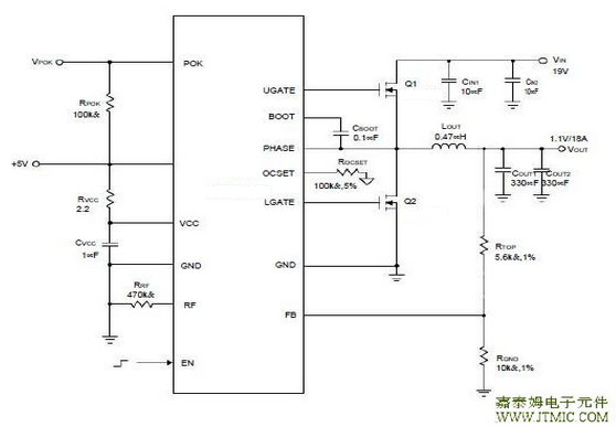
The CXSD62118 is equipped with accurate positive current-limit, output under-voltage, and output over-voltage protections, perfect for NB applications. The Power-On-Reset function monitors the voltage on VCC to prevent wrong operation during power-on. The CXSD62118 has a 1ms digital soft-start and built-in an integrated output discharge method for soft-stop. An internal integrated
soft-start ramps up the output voltage with programmable slew rate to reduce the start-up current. A soft-stop function actively discharges the output capacitors with controlled reverse inductor current.
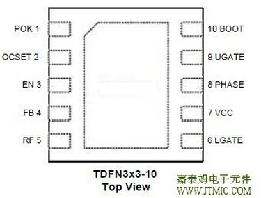
The CXSD62118 is available in 10pin TDFN 3x3 package.
二</span>.产品特点(Features)
Adjustable Output Voltage from +0.7V to +5.5V
- 0.7V Reference Voltage
- ±1% Accuracy Over-Temperature
Operates from an Input Battery Voltage Range of
+1.8V to +28V
Power-On-Reset Monitoring on VCC Pin
Excellent Line and Load Transient Responses
PFM Mode for Increased Light Load Efficiency
Selectable PWM Frequency from 4 Preset Values
Integrated MOSFET Drivers
Integrated Bootstrap Forward P-CH MOSFET
Adjustable Integrated Soft-Start and Soft-Stop
Selectable Forced PWM or Automatic PFM/PWM Mode
Power Good Monitoring
70% Under-Voltage Protection
125% Over-Voltage Protection
Adjustable Current-Limit Protection
- Using Sense Low-Side MOSFET’s RDS(ON)
Over-Temperature Protection
TDFN-10 3x3 Package
Lead Free and Green Devices Available
三</span>,应用范围 (Applications)
Notebook
Table PC
Hand-Held Portable
AIO PC
四.下载产品资料PDF文档
需要详细的PDF规格书请扫一扫微信联系我们,还可以获得免费样品以及技术支持</span>!</span>

七</span>,功能概述
Input Capacitor Selection (Cont.)
higher than the maximum input voltage. The maximum RMS current rating requirement is approximately
IOUT/2,where IOUT is the load current. During power-up, the input capacitors have to handle great
amount of surge current.For low-duty notebook appliactions, ceramic capacitor is recommended. The
capacitors must be connected be-tween the drain of high-side MOSFET and the source of low-side
MOSFET with very low-impeadance PCB layout
MOSFET Selection
The application for a notebook battery with a maximum voltage of 24V, at least a minimum 30V MOSFETs
should be used. The design has to trade off the gate charge with the RDS(ON) of the MOSFET:
For the low-side MOSFET, before it is turned on, the body diode has been conducting. The low-side MOSFET
driver will not charge the miller capacitor of this MOSFET.In the turning off process of the low-side MOSFET,
the load current will shift to the body diode first. The high dv/dt of the phase node voltage will charge the
miller capaci-tor through the low-side MOSFET driver sinking current path. This results in much less switching
loss of the low-side MOSFETs. The duty cycle is often very small in high battery voltage applications, and the
low-side MOSFET will conduct most of the switching cycle; therefore, when using smaller RDS(ON) of the low-side MOSFET, the con-verter can reduce power loss. The gate charge for this MOSFET is usually the
secondary consideration. The high-side MOSFET does not have this zero voltage switch- ing condition;
in addition, because it conducts for less time compared to the low-side MOSFET, the switching
loss tends to be dominant. Priority should be given to the MOSFETs with less gate charge, so
that both the gate driver loss and switching loss will be minimized.
The selection of the N-channel power MOSFETs are determined by the R DS(ON), reversing
transfer capaci-tance (CRSS) and maximum output current requirement. The losses in the
MOSFETs have two components:conduction loss and transition loss. For the high-side and
low-side MOSFETs, the losses are approximately given by the following equations:
Phigh-side = IOUT (1+ TC)(RDS(ON))D + (0.5)( IOUT)(VIN)( tSW)FSW
Plow-side = IOUT (1+ TC)(RDS(ON))(1-D)
Where I is the load current OUT
TC is the temperature dependency of RDS(ON)
FSW is the switching frequency
tSW is the switching interval
D is the duty cycle
Note that both MOSFETs have conduction losses while the high-side MOSFET includes an additional
transition loss.The switching interval, tSW, is the function of the reverse transfer capacitance CRSS.
The (1+TC) term is a factor in the temperature dependency of the RDS(ON) and can be extracted
from the “RDS(ON) vs. Temperature” curve of the power MOSFET.
Layout Consideration
In any high switching frequency converter, a correct layout is important to ensure proper operation
of the regulator.With power devices switching at higher frequency, the resulting current transient will
cause voltage spike across the interconnecting impedance and parasitic circuit elements. As an example,
consider the turn-off transition of the PWM MOSFET. Before turn-off condition, the MOSFET is carrying
the full load current. During turn-off,current stops flowing in the MOSFET and is freewheeling by the
low side MOSFET and parasitic diode. Any parasitic inductance of the circuit generates a large voltage
spike during the switching interval. In general, using short and wide printed circuit traces should
minimize interconnect-ing impedances and the magnitude of voltage spike.
Besides, signal and power grounds are to be kept sepa-rating and finally combined using ground
plane construc-tion or single point grounding. The best tie-point between the signal ground and the
power ground is at the nega-tive side of the output capacitor on each channel, where there is less
noise. Noisy traces beneath the IC are not recommended. Below is a checklist for your layout:
· Keep the switching nodes (UGATE, LGATE, BOOT,and PHASE) away from sensitive small signal
nodes since these nodes are fast moving signals.Therefore, keep traces to these nodes as short as
possible and there should be no other weak signal traces in parallel with theses traces on any layer.
Layout Consideration (Cont.)
· The signals going through theses traces have both high dv/dt and high di/dt with high peak
charging and discharging current. The traces from the gate drivers to the MOSFETs (UGATE and
LGATE) should be short and wide.
· Place the source of the high-side MOSFET and the drain of the low-side MOSFET as close as
possible.Minimizing the impedance with wide layout plane be-tween the two pads reduces the
voltage bounce of the node. In addition, the large layout plane between the drain of the
MOSFETs (VIN and PHASE nodes) can get better heat sinking.
The GND is the current sensing circuit reference ground and also the power ground of the
LGATE low-side MOSFET. On the other hand, the GND trace should be a separate trace and
independently go to the source of the low-side MOSFET. Besides, the cur-rent sense resistor
should be close to OCSET pin to avoid parasitic capacitor effect and noise coupling.
· Decoupling capacitors, the resistor-divider, and boot capacitor should be close to their pins.
(For example,place the decoupling ceramic capacitor close to the drain of the high-side MOSFET
as close as possible.)
· The input bulk capacitors should be close to the drain of the high-side MOSFET, and the output
bulk capaci-tors should be close to the loads. The input capaci-tor’s ground should be close to the
grounds of the output capacitors and low-side MOSFET.
· Locate the resistor-divider close to the FB pin to mini-mize the high impedance trace. In addition,
FB pin traces can’t be close to the switching signal traces (UGATE, LGATE, BOOT, and PHASE).
八,相关产品 更多同类产品......
Switching Regulator > Buck Controller | ||||||||||
Part_No | Package | Archi tectu | Phase | No.of PWM Output | Output Current (A) | Input Voltage (V) | Reference Voltage (V) | Bias Voltage (V) | Quiescent Current (uA) | |
min | max | |||||||||
SOP-14 QSOP-16 QFN4x4-16 | VM | 1 | 1 | 30 | 2.9 | 13.2 | 0.9 | 12 | 8000 | |
SOP-8 | VM | 1 | 1 | 20 | 2.9 | 13.2 | 0.8 | 12 | 5000 | |
SOP-8 | VM | 1 | 1 | 20 | 2.9 | 13.2 | 0.8 | 12 | 5000 | |
QFN4x4-24 | VM | 2 | 1 | 60 | 3.1 | 13.2 | 0.6 | 12 | 5000 | |
SOP-8 | VM | 1 | 1 | 20 | 2.2 | 13.2 | 0.8 | 5~12 | 2100 | |
SOP-8 | VM | 1 | 1 | 20 | 2.2 | 13.2 | 0.8 | 5~12 | 2100 | |
SOP8|TSSOP8 | VM | 1 | 1 | 5 | 5 | 13.2 | 1.25|0.8 | 5~12 | 3000 | |
SOP-8 | VM | 1 | 1 | 10 | 3.3 | 5.5 | 0.8 | 5 | 2100 | |
SOP-14 | VM | 1 | 1 | 10 | 5 | 13.2 | 0.8 | 12 | 2000 | |
TSSOP-24 |QFN5x5-32 | VM | 1 | 2 | 20 | 5 | 13.2 | 0.6 | 5~12 | 4000 | |
SOP14 QSOP16 QFN-16 | VM | 1 | 1 | 30 | 2.9 | 13.2 | 0.9 | 12 | 4000 | |
SOP-14 | VM | 1 | 1 | 30 | 2.2 | 13.2 | 0.6 | 12 | 5000 | |
SOP-14 | VM | 1 | 1 | 30 | 2.2 | 13.2 | 0.6 | 12 | 5000 | |
SOP-14 | VM | 1 | 1 | 25 | 2.2 | 13.2 | 0.8 | 12 | 5000 | |
LQFP7x7 48 TQFN7x7-48 | VM | 1 | 6 | 0.015 | 1.4 | 6.5 | - | 5 | 1800 | |
TSSOP-24P | VM | 1 | 2 | 20 | 2.97 | 5.5 | 0.8 | 5~12 | 5000 | |
SOP-14 | VM | 1 | 1 | 10 | 5 | 13.2 | 0.8 | 12 | 3000 | |
SOP-8-P|DIP-8 | VM | 1 | 1 | 30 | 2.9 | 13.2 | 1.2 | 12 | 3000 | |
SSOP28 QFN4x4-24 | VM | 1 | 2 | 20 | 5 | 24 | 0.9 | 5 | 1200 | |
SOP-20 | VM | 1 | 2 | 20 | 2.2 | 13.2 | 0.6 | 5~12 | 4000 | |
SOP8|DFN3x3-10 | VM | 1 | 2 | - | - | - | - | 5~12 | 550 | |
DIP8|SOP-8 | VM | 1 | 1 | 1 | 1.2 | 9 | 24 | 5 | 9 ~ 24 | |
SSOP16 QFN4x4-16 TQFN3x3-16 | VM | 1 | 1 | 25 | 3 | 25 | 0.6 | 5 | 1700 | |
TDFN3x3-10 | COT | 1 | 1 | 25 | 3 | 25 | 0.5 | 5 | 350 | |
QFN4x4-24 | CM | 2 | 1 | 40 | 4.5 | 13.2 | 0.6 | 5~12 | 4000 | |
SOP8P TDFN3x3-10 | VM | 1 | 1 | 20 | 3 | 13.2 | 0.8 | 5~12 | 2500 | |
SOP8P | VM | 1 | 1 | 25 | 3 | 13.2 | 0.6|0.8 | 5~12 | 1200 | |
TDFN3x3-10 | VM | 1 | 1 | 25 | 4 | 13.2 | 0.8 | 5~12 | 2000 | |
TDFN3x3-10 | COT | 1 | 1 | 25 | 4.5 | 25 | 0.6 | 5~12 | 80 | |
SOP-8P | VM | 1 | 1 | 25 | 4.5 | 13.2 | 0.8 | 5~12 | 16000 | |
TQFN3x3-10 | VM | 1 | 1 | 25 | 4.5 | 13.2 | 0.6 | 5~12 | 2500 | |
TDFN3x3-10 | COT | 1 | 1 | 30 | 3 | 25 | 0.8 | 5~12 | 2000 | |
TQFN3x3-16 | COT | 1 | 1 | 30 | 1.8 | 28 | 0.6 | 5 | 600 | |
TQFN 3x3 16 | COT | 1 | 1 | 30 | 1.8 | 28 | 0.6 | 5 | 600 | |
QFN4x4-24 | VM | 2 | 1 | 50 | 4.5 | 13.2 | 0.6 | 5~12 | 5000 | |
TQFN4x4-24 | COT | 1 | 2 | 15 | 6 | 25 | 2 | N | 550 | |
TQFN4x4-24 | COT | 1 | 2 | 15 | 6 | 25 | 2 | N | 550 | |
TQFN4x4-4 TQFN3x3-20 | COT | 1 | 2 | 20 | 3 | 28 | 0.75 | 5 | 800 | |
TQFN3x3-16 | COT | 1 | 1 | 20 | 1.8 | 28 | 0.75 | 5 | 400 | |
QFN3.5x3.5-14 TQFN3x3-16 | COT | 1 | 1 | 20 | 1.8 | 28 | 0.75 | 5 | 400 | |
TQFN3x3-16 | COT | 1 | 2 | 20 | 1.8 | 28 | 0.75 | 5 | 400 | |
QFN3x3-20 TQFN3x3-16 | COT | 1 | 2 | 20 | 3 | 28 | 1.8|1.5|0.5 | 5 | 740 | |
TQFN4x4-24 |QFN3x3-20 | CM | 1 | 2 | 15 | 5 | 28 | 0.5 | N | 3000 | |
TDFN3x3-10 | COT | 1 | 1 | 20 | 1.8 | 28 | 0.5 | 5 | 250 | |
TQFN3x3-20 | COT | 1 | 2 | 15 | 6 | 25 | 2 | N | 550 | |
TQFN 3x3 20 | COT | 2 | 2 | 11 | 6 | 25 | 2 | N | 550 | |
TQFN3x3-20 | COT | 2 | 2 | 11 | 5.5 | 25 | 2 | N | 280 | |
QFN4x4-24 | VM | 2 | 1 | 60 | 3.1 | 13.2 | 0.85 | 12 | 5000 | |
SOP-8P | VM | 1 | 1 | 20 | 2.9 | 13.2 | 0.8 | 12 | 16000 | |
SOP-20 | VM | 2 | 2 | 30 | 10 | 13.2 | 1 | 12 | 5000 | |
TDFN3x3-10 | COT | 1 | 1 | 25 | 1.8 | 28 | 0.7 | 5 | 250 | |
TQFN3x3-20 | COT | 2 | 1 | 40 | 1.8 | 25 | REFIN Setting | 5 | 700 | |
QFN 3x3 20 TQFN 3x3 16 | COT | 1 | 2 | 20 | 3 | 28 | 1.8|1.5 1.35|1.2 0.5 | 5 | 800 | |
TQFN3x3 20 | COT | 1 | 2 | 15 | 3 | 28 | 0.75 | 5 | 220 | |
TQFN3x3 20 | COT | 1 | 2 | 15 | 3 | 28 | 0.75 | 5 | 220 | |
TQFN3x3-20 | COT | 1 | 2 | 20 | 3 | 28 | 0.75 | 5 | 180 | |


发表评论