
 中文
中文 English
CXSD6279B is a voltage mode and synchronous PWM controller which drives dual N-Channel MOSFETs. It inte-grates the control, monitoring, and protection functions into a single package, provides on
目录
1.产品概述 2.产品特点
3.应用范围 4.下载产品资料PDF文档
5.产品封装图</span> 6.电路原理图</span>
7.功能概述 8.相关产品
一,产品概述(General Description)
The CXSD6279B is a voltage mode and synchronous PWM controller
which drives dual N-Channel MOSFETs. It inte-grates the control, monitoring,
and protection functions into a single package, provides one controlled power
outputs with under-voltage and over-current protection.CXSD6279B provides
excellent regulation for output load variation. An internal 0.8V temperature-
compensated reference voltage is designed to meet the requirement of
low output voltage applications. It includes a 200kHz free-running
triangle-wave oscillator that is adjustable from 70kHz to 800kHz.
The power-on-reset (POR) circuit monitors the VCC, EN,and OCSET
input voltage to start-up or shutdown the IC.The over-current protection (OCP)
monitors the output current by using the voltage drop across the upper
MOSFET’s RDS(ON), eliminating the need for a current sens-ing resistor.
The under-voltage protection (UVP) moni-tors the voltage of the FB pin for
short-circuit protection.The over-current protection trip cycle the soft-start
func-tion until the fault events be removed. Under-voltage pro-tection will
shutdown the IC directly.
二</span>.产品特点(Features)
1.)Simple Single-Loop Control Design
Voltage-Mode PWM Control
2.)Fast Transient Response
Full 0–100% Duty Ratio
3.)Excellent Output Voltage Regulation
0.8V Internal Reference
± 1% Over Line Voltage and Temperature
4.)Over Current Fault Monitor
Uses Upper MOSFETs RDS (ON)
5.)Converter Can Source and Sink Current
6.)Small Converter Size
200kHz Free-Running Oscillator
Programmable from 70kHz to 800kHz
7.)14-Lead SOIC Package
8.)Lead Free and Green Devices Available (RoHS Compliant)
三</span>,应用范围 (Applications)
Graphic Cards
DDR Memory Power Supply
DDR Memory Termination Voltage
Low-Voltage Distributed Power Supplies
四.下载产品资料PDF文档
需要详细的PDF规格书请扫一扫微信联系我们,还可以获得免费样品以及技术支持</span>!</span>


RT (Pin1)
This pin can adjust the switching frequency. Connect a resistor from the RT to the GND for increasing the switch-
OCSET (Pin2)
This pin serves two functions: a shutdown control and the setting of over current-limit threshold. Pulling this pin
below 1.27V will shutdown the controller, forcing the UGATE and LGATE signals to be at 0V.
A resistor (Rocset) connected between this pin and the drain of the high side MOSFET will determine the over
current limit. An internal 200μA current source will flow through this resistor, creating a voltage drop, which
will be com-pared with the voltage across the high side MOSFET.
SS (Pin3)
Connect a capacitor from the pin to the GND to set the soft-start interval of the converter. An internal 10μA
current source charges this capacitor to 5.8V. The SS voltage clamps the error amplifier output, and Figure1
shows the soft-start interval. At t1, the SS voltage reaches the valley of the oscillator’s triangle wave. The
PWM comparator starts to generate a PWM signal to control logic, and the
COMP (Pin4)
This pin is the output of the error amplifier. Add an exter-nal resistor and capacitor network to provide the
loop com- pensation for the PW M converter (see Application Information).
FB (Pin5)
FB pin is the inverter input of the error amplifier and it receives the feedback voltage from an external
resis-tive divider across the output (V OUT). The output voltage is determined by:
EN (Pin6)
Pull the pin higher than 2V to enable the device, and pull the pin lower than 0.8V to shutdown the
device. In shutdown, the SS is discharged and the UGATE and LGATE pins are held low. The EN pin
is the open-collector, and it will not be floating.
GND (Pin7)
Signal ground for the IC.
PHASE (Pin8)
This pin is connected to the source of the high-side MOSFET and is used to monitor the voltage drop
across the high-side MOSFET for over-current protection.
UGATE (Pin9)
Connect the pin to external MOSFET, and provides the gate drive for the upper MOSFET.
BOOT (Pin 10)
This pin provides the supply voltage to the high side MOSFET driver. For driving logic level N-channel
MOSEFT,a bootstrap circuit can be used to create a suitable driver’s supply.
PGND (Pin11)
Power ground for the gate diver. Connect the lower MOSFET source to this pin.
LGATE (Pin 12)
Connect the pin to the external MOSFET, and provides the gate drive signal for the lower MOSFET.
PVCC (Pin13)
This pin provides a supply voltage for the lower gate drive, connect it to the VCC pin in common use.
VCC (Pin14)
This pin provides a supply voltage for the device. When the VCC is above the rising threshold 10.4V,
the device is turned on; conversely, when the VCC is below the falling threshold, the device is turned off.
六.电路原理图</span>
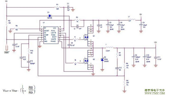
七</span>,功能概述
Output Capacitor Selection
The selection of COUT is determined by the required effec-tive series resistance (ESR) and voltage rating
rather than the actual capacitance requirement. Therefore, select highperformance low ESR capacitors
that are intended for switching regulator applications. In some applications,multiple capacitors have to
be paralled to achieve the desired ESR value. If tantalum capacitors are used, makesure they are surge
tested by the manufactures. If in doubt,consult the capacitors manufacturer.
Input Capacitor Selection
The input capacitor is chosen based on the voltage rating and the RMS current rating. For reliable
operation, select the capacitor voltage rating to be at least 1.3 times higher than the maximum input
voltage. The maximum RMS current rating requirement is approximately IOUT/2 , where IOUT is the
load current. During power up, the input capaci-tors have to handle large amount of surge current.
If tanta-lum capacitors are used, make sure they are surge tested by the manufactures. If in doubt,
consult the capacitors manufacturer.For high frequency decoupling, a ceramic capacitor be-tween
0.1μF to 1μF can be connected between the VCC and the ground pin.
Inductor Selection
The inductance of the inductor is determined by the out-put voltage requirement. The larger the
inductance, the lower the inductor’s current ripple. This will translate into lower output ripple voltage.
The ripple current and ripple voltage can be approximated by:
where Fs is the switching frequency of the regulator.There is a tradeoff exists between the inductor’s
ripple current and the regulator load transient response time. A smaller inductor will give the regulator
a faster load tran-sient response at the expense of higher ripple current and vice versa. The maximum
ripple current occurs at the maximum input voltage. A good starting point is to choose the ripple
current to be approximately 30% of the maxi-mum output current.Once the inductance value has
been chosen, select an inductor that is capable of carrying the required peak cur-rent without going
into saturation. In some types of inductors, especially core that is make of ferrite, the ripple
current will increase abruptly when it saturates. This will result in a larger output ripple voltage.
Compensation
The output LC filter introduces a double pole, which con-tributes with –40dB/decade gain slope and
180 degrees phase shift in the control loop. A compensation network between the COMP pin and the
ground should be added. The simplest loop compensation network is shown in
Figure 5.
The output LC filter consists of the output inductor and output capacitors. The transfer function of
the LC filter is given by:
八,相关产品 更多同类产品......
Switching Regulator > Buck Controller | ||||||||||
Part_No | Package | Archi tectu | Phase | No.of PWM Output | Output Current (A) | Input Voltage (V) | Reference Voltage (V) | Bias Voltage (V) | Quiescent Current (uA) | |
min | max | |||||||||
SOP-14 QSOP-16 QFN4x4-16 | VM | 1 | 1 | 30 | 2.9 | 13.2 | 0.9 | 12 | 8000 | |
SOP-8 | VM | 1 | 1 | 20 | 2.9 | 13.2 | 0.8 | 12 | 5000 | |
SOP-8 | VM | 1 | 1 | 20 | 2.9 | 13.2 | 0.8 | 12 | 5000 | |
QFN4x4-24 | VM | 2 | 1 | 60 | 3.1 | 13.2 | 0.6 | 12 | 5000 | |
SOP-8 | VM | 1 | 1 | 20 | 2.2 | 13.2 | 0.8 | 5~12 | 2100 | |
SOP-8 | VM | 1 | 1 | 20 | 2.2 | 13.2 | 0.8 | 5~12 | 2100 | |
SOP8|TSSOP8 | VM | 1 | 1 | 5 | 5 | 13.2 | 1.25|0.8 | 5~12 | 3000 | |
SOP-8 | VM | 1 | 1 | 10 | 3.3 | 5.5 | 0.8 | 5 | 2100 | |
SOP-14 | VM | 1 | 1 | 10 | 5 | 13.2 | 0.8 | 12 | 2000 | |
TSSOP-24 |QFN5x5-32 | VM | 1 | 2 | 20 | 5 | 13.2 | 0.6 | 5~12 | 4000 | |
SOP14 QSOP16 QFN-16 | VM | 1 | 1 | 30 | 2.9 | 13.2 | 0.9 | 12 | 4000 | |
SOP-14 | VM | 1 | 1 | 30 | 2.2 | 13.2 | 0.6 | 12 | 5000 | |
SOP-14 | VM | 1 | 1 | 30 | 2.2 | 13.2 | 0.6 | 12 | 5000 | |
SOP-14 | VM | 1 | 1 | 25 | 2.2 | 13.2 | 0.8 | 12 | 5000 | |
LQFP7x7 48 TQFN7x7-48 | VM | 1 | 6 | 0.015 | 1.4 | 6.5 | - | 5 | 1800 | |
TSSOP-24P | VM | 1 | 2 | 20 | 2.97 | 5.5 | 0.8 | 5~12 | 5000 | |
SOP-14 | VM | 1 | 1 | 10 | 5 | 13.2 | 0.8 | 12 | 3000 | |
SOP-8-P|DIP-8 | VM | 1 | 1 | 30 | 2.9 | 13.2 | 1.2 | 12 | 3000 | |
SSOP28 QFN4x4-24 | VM | 1 | 2 | 20 | 5 | 24 | 0.9 | 5 | 1200 | |
SOP-20 | VM | 1 | 2 | 20 | 2.2 | 13.2 | 0.6 | 5~12 | 4000 | |
SOP8|DFN3x3-10 | VM | 1 | 2 | - | - | - | - | 5~12 | 550 | |
DIP8|SOP-8 | VM | 1 | 1 | 1 | 1.2 | 9 | 24 | 5 | 9 ~ 24 | |
SSOP16 QFN4x4-16 TQFN3x3-16 | VM | 1 | 1 | 25 | 3 | 25 | 0.6 | 5 | 1700 | |
TDFN3x3-10 | COT | 1 | 1 | 25 | 3 | 25 | 0.5 | 5 | 350 | |
QFN4x4-24 | CM | 2 | 1 | 40 | 4.5 | 13.2 | 0.6 | 5~12 | 4000 | |
SOP8P TDFN3x3-10 | VM | 1 | 1 | 20 | 3 | 13.2 | 0.8 | 5~12 | 2500 | |
SOP8P | VM | 1 | 1 | 25 | 3 | 13.2 | 0.6|0.8 | 5~12 | 1200 | |
TDFN3x3-10 | VM | 1 | 1 | 25 | 4 | 13.2 | 0.8 | 5~12 | 2000 | |
TDFN3x3-10 | COT | 1 | 1 | 25 | 4.5 | 25 | 0.6 | 5~12 | 80 | |
SOP-8P | VM | 1 | 1 | 25 | 4.5 | 13.2 | 0.8 | 5~12 | 16000 | |
TQFN3x3-10 | VM | 1 | 1 | 25 | 4.5 | 13.2 | 0.6 | 5~12 | 2500 | |
TDFN3x3-10 | COT | 1 | 1 | 30 | 3 | 25 | 0.8 | 5~12 | 2000 | |
TQFN3x3-16 | COT | 1 | 1 | 30 | 1.8 | 28 | 0.6 | 5 | 600 | |
TQFN 3x3 16 | COT | 1 | 1 | 30 | 1.8 | 28 | 0.6 | 5 | 600 | |
QFN4x4-24 | VM | 2 | 1 | 50 | 4.5 | 13.2 | 0.6 | 5~12 | 5000 | |
TQFN4x4-24 | COT | 1 | 2 | 15 | 6 | 25 | 2 | N | 550 | |
TQFN4x4-24 | COT | 1 | 2 | 15 | 6 | 25 | 2 | N | 550 | |
TQFN4x4-4 TQFN3x3-20 | COT | 1 | 2 | 20 | 3 | 28 | 0.75 | 5 | 800 | |
TQFN3x3-16 | COT | 1 | 1 | 20 | 1.8 | 28 | 0.75 | 5 | 400 | |
QFN3.5x3.5-14 TQFN3x3-16 | COT | 1 | 1 | 20 | 1.8 | 28 | 0.75 | 5 | 400 | |
TQFN3x3-16 | COT | 1 | 2 | 20 | 1.8 | 28 | 0.75 | 5 | 400 | |
QFN3x3-20 TQFN3x3-16 | COT | 1 | 2 | 20 | 3 | 28 | 1.8|1.5|0.5 | 5 | 740 | |
TQFN4x4-24 |QFN3x3-20 | CM | 1 | 2 | 15 | 5 | 28 | 0.5 | N | 3000 | |
TDFN3x3-10 | COT | 1 | 1 | 20 | 1.8 | 28 | 0.5 | 5 | 250 | |
TQFN3x3-20 | COT | 1 | 2 | 15 | 6 | 25 | 2 | N | 550 | |
TQFN 3x3 20 | COT | 2 | 2 | 11 | 6 | 25 | 2 | N | 550 | |
TQFN3x3-20 | COT | 2 | 2 | 11 | 5.5 | 25 | 2 | N | 280 | |
QFN4x4-24 | VM | 2 | 1 | 60 | 3.1 | 13.2 | 0.85 | 12 | 5000 | |
SOP-8P | VM | 1 | 1 | 20 | 2.9 | 13.2 | 0.8 | 12 | 16000 | |
SOP-20 | VM | 2 | 2 | 30 | 10 | 13.2 | 1 | 12 | 5000 | |
TDFN3x3-10 | COT | 1 | 1 | 25 | 1.8 | 28 | 0.7 | 5 | 250 | |
TQFN3x3-20 | COT | 2 | 1 | 40 | 1.8 | 25 | REFIN Setting | 5 | 700 | |
QFN 3x3 20 TQFN 3x3 16 | COT | 1 | 2 | 20 | 3 | 28 | 1.8|1.5 1.35|1.2 0.5 | 5 | 800 | |
TQFN3x3 20 | COT | 1 | 2 | 15 | 3 | 28 | 0.75 | 5 | 220 | |
TQFN3x3 20 | COT | 1 | 2 | 15 | 3 | 28 | 0.75 | 5 | 220 | |
TQFN3x3-20 | COT | 1 | 2 | 20 | 3 | 28 | 0.75 | 5 | 180 | |


发表评论