The CXSU63137 integrates with a high-performance step-up converter, two linear-regulator controllers, a high voltage switch and one (CXSU63137), three (CXSU63137-1) or five (CXSU63137-2)

发布时间:2020-04-06 09:43:38 浏览次数:714 作者:嘉泰姆 来源:1
摘要:The CXSU63137 integrates with a high-performance step-up converter, two linear-regulator controllers, a high voltage switch and one (CXSU63137), three (CXSU63137-1) or five (CXSU63137-2)

目录Dzt嘉泰姆

1.产品概述                       2.产品特点
3.应用范围                       4.下载产品资料PDF文档 
5.产品封装图</span>                     6.电路原理图</span>                   
7.
功能概述
                        8.相关产品Dzt嘉泰姆

一,产品概述(General Description)         Dzt嘉泰姆


           The CXSU63137 integrates with a high-performance step-up converter, two linear-regulator controllers, a high voltage switch and one (CXSU63137), three (CXSU63137) or five (CXSU63137) high current operational amplifiers for TFT-LCD applications.The main step-up regulator is a current-mode, fixed-fre-quency PWM switching regulator. The 1.2MHz switching frequency allows the usage of low-profile inductors and ceramic capacitors to minimize the thickness of LCD panel designs.
      The linear-regulator controllers used external transistors provide regulated the gate-driver of TFT-LCD VGON and VGOFF supplies.
The amplifiers are ideal for VCOM and VGAMMA applications, with
150m A peak output current drive, 10MHz bandwidth, and 13V/μs slew
rate. All inputs and outputs are rail-to-rail.
     The CXSU63137/1/2 is available in a tiny 5mm x 5mm 32-pin QFN package (TQFN5x5-32).

二.产品特点(Features)Dzt嘉泰姆


· 2.6V to 6.5V Input Supply Range Dzt嘉泰姆

· Current-Mode Step-Up Regulator Dzt嘉泰姆

 - Fast Transient Response Dzt嘉泰姆

 - 1.2MHz Fixed Operating Frequency Dzt嘉泰姆

· ±1.5% High-Accuracy Output Voltage Dzt嘉泰姆

· 3A, 20V, 0.25W Internal N-Channel MOSFET Dzt嘉泰姆

· High Efficiency Dzt嘉泰姆

· Low Quiescent Current (0.6mA Typical) Dzt嘉泰姆

· Linear-Regulator Controllers for VGON and VGOFF Dzt嘉泰姆

· High-performance Operational Amplifiers Dzt嘉泰姆

 - ±150mA Output Short-Circuit CurrentDzt嘉泰姆

 - 13V/ms Slew Rate - 10MHz, -3dB Bandwidth Dzt嘉泰姆

 - Rail-to-Rail Inputs/Outputs Dzt嘉泰姆

· Fault-Delay Timer and Fault Latch for All Regulator Outputs Dzt嘉泰姆

· Over-Temperature Protection Dzt嘉泰姆

· Available in Compact 32-pin 5mmx5mm Thin QFN Package (TQFN5x5-32) Dzt嘉泰姆

· Lead Free Available (RoHS Compliant)
Dzt嘉泰姆

三</span>,应用范围 (Applications)Dzt嘉泰姆


    TFT LCD Displays for Monitors
   TFT LCD Displays for Notebook Computers
   Automotive Displays

四.下载产品资料PDF文档 
Dzt嘉泰姆


需要详细的PDF规格书请扫一扫微信联系我们,还可以获得免费样品以及技术支持</span>!</span>

Dzt嘉泰姆

 QQ截图20160419174301.jpgDzt嘉泰姆

五,产品封装图 (Package)Dzt嘉泰姆


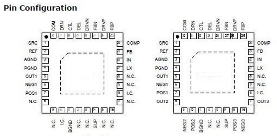
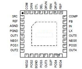
blob.pngblob.pngPin Function Description
Dzt嘉泰姆

PinDzt嘉泰姆

NameDzt嘉泰姆

Function DescriptionDzt嘉泰姆

CXSU63137Dzt嘉泰姆

CXSU63137-1Dzt嘉泰姆

CXSU63137-2Dzt嘉泰姆

1Dzt嘉泰姆

SRCDzt嘉泰姆

SRCDzt嘉泰姆

SRCDzt嘉泰姆

Switch Input. Source of the internal high-voltage P-channel MOSFET. Bypass
SRC to PGND with a minimum of 0.1μF capacitor closed to the pins.Dzt嘉泰姆

2Dzt嘉泰姆

REFDzt嘉泰姆

REFDzt嘉泰姆

REFDzt嘉泰姆

Reference voltage output. Bypass REF to AGND with a minimum of
0.22μFcapacitor closed to the pins.Dzt嘉泰姆

3Dzt嘉泰姆

AGNDDzt嘉泰姆

AGNDDzt嘉泰姆

AGNDDzt嘉泰姆

Analog Ground for Step-Up Regulator and Linear Regulators. Connect to
power ground (PGND) underneath the IC.Dzt嘉泰姆

4Dzt嘉泰姆

PGNDDzt嘉泰姆

PGNDDzt嘉泰姆

PGNDDzt嘉泰姆

Power Ground for Step-Up Regulator. PGND is the source of the main step-up
n-channel power MOSFET. Connect PGND to the ground terminals of output
capacitors through a short, wide PC board trace. Connect to analog ground
(AGND) underneath the IC.Dzt嘉泰姆

5Dzt嘉泰姆

OUT1Dzt嘉泰姆

OUT1Dzt嘉泰姆

OUT1Dzt嘉泰姆

Output of Operational-Amplifier 1Dzt嘉泰姆

6Dzt嘉泰姆

NEG1Dzt嘉泰姆

NEG1Dzt嘉泰姆

NEG1Dzt嘉泰姆

Inverting Input of Operational-Amplifier 1Dzt嘉泰姆

7Dzt嘉泰姆

POS1Dzt嘉泰姆

POS1Dzt嘉泰姆

POS1Dzt嘉泰姆

Non-inverting Input of Operational-Amplifier 1Dzt嘉泰姆

8Dzt嘉泰姆

NCDzt嘉泰姆

OUT2Dzt嘉泰姆

OUT2Dzt嘉泰姆

Output of Operational-Amplifier 2 of CXSU63137/CXSU63137. No internal
connected of CXSU63137.Dzt嘉泰姆

9Dzt嘉泰姆

NCDzt嘉泰姆

NEG2Dzt嘉泰姆

NEG2Dzt嘉泰姆

Inverting Input of Operational-Amplifier 2 of CXSU63137/CXSU63137. No internal
connected of CXSU63137.Dzt嘉泰姆

10Dzt嘉泰姆

ICDzt嘉泰姆

POS2Dzt嘉泰姆

POS2Dzt嘉泰姆

Non-inverting Input of Operational-Amplifier 2 of CXSU63137/CXSU63137. Internal
connected to GND of CXSU63137Dzt嘉泰姆

11Dzt嘉泰姆

BGNDDzt嘉泰姆

BGNDDzt嘉泰姆

BGNDDzt嘉泰姆

Analog Ground for Operational Amplifiers. Connect to power ground (PGND)
underneath the IC.Dzt嘉泰姆

12Dzt嘉泰姆

NCDzt嘉泰姆

NCDzt嘉泰姆

POS3Dzt嘉泰姆

Non-inverting Input of Operational-Amplifier 3 of CXSU63137. No internal
connected of CXSU63137/CXSU63137.Dzt嘉泰姆

13Dzt嘉泰姆

NCDzt嘉泰姆

NCDzt嘉泰姆

OUT3Dzt嘉泰姆

Output of Operational-Amplifier 3 of CXSU63137. No internal connected ofCXSU63137/CXSU63137.Dzt嘉泰姆

14Dzt嘉泰姆

SUPDzt嘉泰姆

SUPDzt嘉泰姆

SUPDzt嘉泰姆

Power Input of Operational Amplifiers. Typically connected to VMAIN. Bypass
SUP to BGND with a 0.1μF capacitor.Dzt嘉泰姆

15Dzt嘉泰姆

NCDzt嘉泰姆

POS3Dzt嘉泰姆

POS4Dzt嘉泰姆

Non-inverting Input of Operational-Amplifier 4 of CXSU63137. Non-inverting
Input of Operational-Amplifier 3 of CXSU63137. No internal connected ofCXSU63137.Dzt嘉泰姆

16Dzt嘉泰姆

NCDzt嘉泰姆

NEG3Dzt嘉泰姆

NEG4Dzt嘉泰姆

Inverting Input of Operational-Amplifier 4 of CXSU63137. Inverting Input of
Operational-Amplifier 3 of CXSU63137. No internal connected of CXSU63137.Dzt嘉泰姆

17Dzt嘉泰姆

NCDzt嘉泰姆

OUT3Dzt嘉泰姆

OUT4Dzt嘉泰姆

Output of Operational-Amplifier 4 of CXSU63137. Output of
Operational-Amplifier 3 of CXSU63137. No internal connected of CXSU63137.Dzt嘉泰姆

18Dzt嘉泰姆

ICDzt嘉泰姆

ICDzt嘉泰姆

POS5Dzt嘉泰姆

Non-inverting Input of Operational-Amplifier 5 of CXSU63137. Internal connected
to GND of CXSU63137/CXSU63137.Dzt嘉泰姆

19Dzt嘉泰姆

NCDzt嘉泰姆

NCDzt嘉泰姆

NEG5Dzt嘉泰姆

Inverting Input of Operational-Amplifier 5 of CXSU63137. No internal connected
of CXSU63137/CXSU63137.Dzt嘉泰姆

20Dzt嘉泰姆

NCDzt嘉泰姆

NCDzt嘉泰姆

OUT5Dzt嘉泰姆

Output of Operational-Amplifier 5 of CXSU63137. No internal connected ofCXSU63137/CXSU63137.Dzt嘉泰姆

21Dzt嘉泰姆

LXDzt嘉泰姆

LXDzt嘉泰姆

LXDzt嘉泰姆

N-Channel Power MOSFET Drain and Switching Node. Connect the inductor
and Schottky diode to LX and minimize the trace area for lowest EMI.Dzt嘉泰姆

22Dzt嘉泰姆

INDzt嘉泰姆

INDzt嘉泰姆

INDzt嘉泰姆

Supply Voltage Input. Bypass IN to AGND with a 0.1μF capacitor. IN can range
from 2.6V to 6.5V.Dzt嘉泰姆

23Dzt嘉泰姆

FBDzt嘉泰姆

FBDzt嘉泰姆

FBDzt嘉泰姆

Step-Up Regulator Feedback Input. Connect a resistive voltage-divider from
the output (VMAIN) to FB to analog ground (AGND). Place the divider within
5mm of FB.Dzt嘉泰姆

24Dzt嘉泰姆

COMPDzt嘉泰姆

COMPDzt嘉泰姆

COMPDzt嘉泰姆

Step-Up Regulator Error-Amplifier Compensation Point. Connect a series RC
from COMP to AGND.Dzt嘉泰姆

PinFunction Description
Dzt嘉泰姆

PinDzt嘉泰姆

NameDzt嘉泰姆

Function DescriptionDzt嘉泰姆

CXSU63137Dzt嘉泰姆

CXSU63137-1Dzt嘉泰姆

CXSU63137-2Dzt嘉泰姆

24Dzt嘉泰姆

COMPDzt嘉泰姆

COMPDzt嘉泰姆

COMPDzt嘉泰姆

Step-Up Regulator Error-Amplifier Compensation Point. Connect a series RC
from COMP to AGND.Dzt嘉泰姆

25Dzt嘉泰姆

FBPDzt嘉泰姆

FBPDzt嘉泰姆

FBPDzt嘉泰姆

Gate-On Linear-Regulator Feedback Input. Connect FBP to the center of a
resistive voltage-divider between the regulator output and AGND to set the
gate-on linear regulator output voltage. Place the resistive voltage-divider
close to the pin.Dzt嘉泰姆

26Dzt嘉泰姆

DRVPDzt嘉泰姆

DRVPDzt嘉泰姆

DRVPDzt嘉泰姆

Gate-On Linear-Regulator Base Drive. Open drain of an internal n-channel
MOSFET. Connect DRVP to the base of an external PNP pass transistor.Dzt嘉泰姆

27Dzt嘉泰姆

FBNDzt嘉泰姆

FBNDzt嘉泰姆

FBNDzt嘉泰姆

Gate-Off Linear-Regulator Feedback Input. Connect FBN to the center of a
resistive voltage-divider between the regulator output and REF to set the
gate-off linear regulator output voltage. Place the resistive voltage-divider
close to the pin.Dzt嘉泰姆

28Dzt嘉泰姆

DRVNDzt嘉泰姆

DRVNDzt嘉泰姆

DRVNDzt嘉泰姆

Gate-Off Linear-Regulator Base Drive. Open drain of an internal p-channel
MOSFET. Connect DRVN to the base of an external NPN pass transistor.Dzt嘉泰姆

29Dzt嘉泰姆

DELDzt嘉泰姆

DELDzt嘉泰姆

DELDzt嘉泰姆

High-Voltage Switch Delay Input. Connect a capacitor from DEL to AGND to
set the high-voltage switch startup delay.Dzt嘉泰姆

30Dzt嘉泰姆

CTLDzt嘉泰姆

CTLDzt嘉泰姆

CTLDzt嘉泰姆

High-Voltage Switch Control Input. When CTL is high, the high-voltage switch
between COM and SRC is on and the high-voltage switch between COM and
DRN is off. When CTL is low, the high-voltage switch between COM and SRC
is off and the high-voltage switch between COM and DRN is on. CTL is
inhibited by the undervoltage lockout and when the voltage on DEL is less than
1.25V.Dzt嘉泰姆

31Dzt嘉泰姆

DRNDzt嘉泰姆

DRNDzt嘉泰姆

DRNDzt嘉泰姆

Switch Input. Drain of the internal high-voltage back-to-back P-channel
MOSFETs connected to COM. Do not allows the voltage on DRN to exceed
VSRC.Dzt嘉泰姆

32Dzt嘉泰姆

COMDzt嘉泰姆

COMDzt嘉泰姆

COMDzt嘉泰姆

Internal High-Voltage MOSFET Switch Common Terminal. Do not allow the
voltage on COM to exceed VSRC.Dzt嘉泰姆

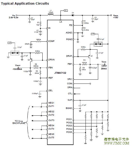
六.电路原理图</span>Dzt嘉泰姆


七</span>,功能概述
For all switching power supplies, the layout is an impor-tant step in the design; especially at high peak currents and switching frequencies. There are some general guidelines for layout:
1.Place the external power components (the input capacitors, output capacitors, boost inductor and output diodes, etc.) in close proximity to the device.Traces to these components should be kept as short and wide as possible to minimize parasitic inductance and resistance.
2.Place the REF and IN bypass capacitors close to the pins. The ground connection of the IN bypass capacitor should be connected directly to the AGND pin with a wide trace.
3.Create a power ground (PGND) and a signal ground island and connect at only one point. The power ground consisting of the input and output capacitor grounds, PGND pin, and any charge-pump components. Connect all of these together with short, wide traces or a small ground plane. Maxi-mizing the width of the power ground traces im-proves efficiency and reduces output voltage ripple and noise spikes. The analog ground plane (AGND) consisting of the AGND pin, all the feed-back-divider ground connections, the operational-amplifier divider ground connections, the COMP and DEL capacitor ground connections, and the device’s exposed backside pad. Connect the AGND and PGND islands by connecting the PGND pin directly to the exposed backside pad. Make no other connections between these separate ground planes.
4.The feedback network should sense the output volt-age directly from the point of load, and be as far away from LX node as possible.
5.The exposed die plate, underneath the package,should be soldered to an equivalent area of metal on the PCB. This contact area should have mul-tiple via connections to the back of the PCB as well as connections to intermediate PCB layers, if available, to maximize thermal dissipation away from the IC.
6.To minimize the thermal resistance of the package when soldered to a multi-layer PCB, the amount of copper track and ground plane area connected to the exposed die plate should be maximized and spread out as far as possible from the IC. The bot-tom and top PCB areas especially should be maxi-mized to allow thermal dissipation to the surround-ing air.
7.Minimize feedback input track lengths to avoid switching noise pick-up
八,相关产品
Dzt嘉泰姆

Dzt嘉泰姆

Switching Regulator > Boost ConverterDzt嘉泰姆

 Part_No Dzt嘉泰姆

PackageDzt嘉泰姆

Archi-tecture Dzt嘉泰姆

Input Dzt嘉泰姆

Voltage    Dzt嘉泰姆

Max Adj.Dzt嘉泰姆

Output Dzt嘉泰姆

Voltage Dzt嘉泰姆

Switch Current Limit (max) Dzt嘉泰姆

Fixed Dzt嘉泰姆

Output Dzt嘉泰姆

Voltage  Dzt嘉泰姆

Switching Dzt嘉泰姆

Frequency Dzt嘉泰姆

Internal Power   Switch Dzt嘉泰姆

Sync. Rectifier Dzt嘉泰姆


minDzt嘉泰姆

maxDzt嘉泰姆

minDzt嘉泰姆

maxDzt嘉泰姆

(A)Dzt嘉泰姆

(V)Dzt嘉泰姆

(kHz)Dzt嘉泰姆


CXSU63133Dzt嘉泰姆

SOT89Dzt嘉泰姆

VM Dzt嘉泰姆

0.9Dzt嘉泰姆

5.5Dzt嘉泰姆

2.5Dzt嘉泰姆

5.5Dzt嘉泰姆

0.5Dzt嘉泰姆

1.8|2.6|2.8|3Dzt嘉泰姆

|3.3|3.8|4.5|5Dzt嘉泰姆

-Dzt嘉泰姆

NoDzt嘉泰姆

YesDzt嘉泰姆

CXSU63134Dzt嘉泰姆

MSOP8|TSSOP8Dzt嘉泰姆

|SOP8Dzt嘉泰姆

VMDzt嘉泰姆

2.5Dzt嘉泰姆

5.5Dzt嘉泰姆

2.5Dzt嘉泰姆

-Dzt嘉泰姆

-Dzt嘉泰姆

-Dzt嘉泰姆

200 ~ 1000Dzt嘉泰姆

NoDzt嘉泰姆

NoDzt嘉泰姆

CXSU63135Dzt嘉泰姆

TSSOP8|SOP-8PDzt嘉泰姆

VMDzt嘉泰姆

1Dzt嘉泰姆

5.5Dzt嘉泰姆

2.5Dzt嘉泰姆

5Dzt嘉泰姆

1Dzt嘉泰姆

2.5|3.3Dzt嘉泰姆

300Dzt嘉泰姆

YesDzt嘉泰姆

YesDzt嘉泰姆

CXSU63136Dzt嘉泰姆

SOP8Dzt嘉泰姆

CMDzt嘉泰姆

3Dzt嘉泰姆

40Dzt嘉泰姆

1.25Dzt嘉泰姆

40Dzt嘉泰姆

1.5Dzt嘉泰姆

-Dzt嘉泰姆

33 ~ 100Dzt嘉泰姆

YesDzt嘉泰姆

NoDzt嘉泰姆

CXSU63137Dzt嘉泰姆

TQFN5x5-32Dzt嘉泰姆

CMDzt嘉泰姆

2.5Dzt嘉泰姆

6.5Dzt嘉泰姆

2.5Dzt嘉泰姆

18Dzt嘉泰姆

3Dzt嘉泰姆

NoDzt嘉泰姆

1200Dzt嘉泰姆

YesDzt嘉泰姆

NoDzt嘉泰姆

CXSU63138Dzt嘉泰姆

TSOT23-5Dzt嘉泰姆

TDFN2x2-6Dzt嘉泰姆

CMDzt嘉泰姆

2.5Dzt嘉泰姆

6Dzt嘉泰姆

2.5Dzt嘉泰姆

20Dzt嘉泰姆

2Dzt嘉泰姆

-Dzt嘉泰姆

1500Dzt嘉泰姆

YesDzt嘉泰姆

NoDzt嘉泰姆

CXSU63139Dzt嘉泰姆

TQFN4x4-6Dzt嘉泰姆

TDFN3x3-12Dzt嘉泰姆

CMDzt嘉泰姆

1.8Dzt嘉泰姆

5.5Dzt嘉泰姆

2.7Dzt嘉泰姆

5.5Dzt嘉泰姆

5Dzt嘉泰姆

-Dzt嘉泰姆

1.2Dzt嘉泰姆

YesDzt嘉泰姆

YesDzt嘉泰姆

CXSU63140Dzt嘉泰姆

SOT23-5Dzt嘉泰姆

CMDzt嘉泰姆

2.5Dzt嘉泰姆

6Dzt嘉泰姆

2.5Dzt嘉泰姆

32Dzt嘉泰姆

1Dzt嘉泰姆

-Dzt嘉泰姆

1000Dzt嘉泰姆

YesDzt嘉泰姆

NoDzt嘉泰姆

CXSU63141Dzt嘉泰姆

TSOT-23-6 Dzt嘉泰姆

TDFN2x2-8Dzt嘉泰姆

CMDzt嘉泰姆

1.2Dzt嘉泰姆

5.5Dzt嘉泰姆

1.8Dzt嘉泰姆

5.5Dzt嘉泰姆

1.2Dzt嘉泰姆

-Dzt嘉泰姆

1.2Dzt嘉泰姆

YesDzt嘉泰姆

YesDzt嘉泰姆


Dzt嘉泰姆

文章标签

暂无标签

发表评论

共有条评论
用户名: 密码:
验证码: 匿名发表

AI 智能助手