目录aA7嘉泰姆
1.产品概述 2.产品特点
3.应用范围 4.下载产品资料PDF文档
5.产品封装图</span> 6.电路原理图</span>
7.功能概述 8.相关产品aA7嘉泰姆
一,产品概述(General Description) aA7嘉泰姆
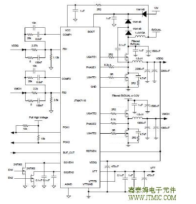
The CXSD6285 integrates Dual PWM buck controllers and an internal linear regulator for DDR memory and MCH power solution. The two synchronous PWM buck control-lers drive four N-channel MOSFETs for DDR memory sup-ply voltage (VDDQ) and MCH regulator. The internal regu-lator is designed to track at the half of the reference volt-age with sourcing and sinking current for DDR memory termination regulator (VTT).
The CXSD6285 uses the latched BUF_Cut signal and the POR of the BOOT to comply with ACPI power sequencing specifications. The two PWM regulators also provide POKsignals to indicate that the regulators are good. The de-vice also has the phase shift function between the two PWM controllers. The protection functions of the two PWM controllers include over-current protection, under-voltage protection, and external soft-start function. The VTT regu-lator provides 2A sinking and sourcing current-limit func-tion and also has thermal shutdown protection.
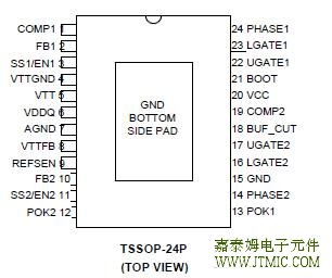
The TSSOP-24P package with a copper pad provides excellent thermal impedance is available.
二</span>.产品特点(Features)aA7嘉泰姆
1.)Provide Synchronous Rectified Buck PWM Controllers for VDDQ and VMCH
2.)</strong>Integrated Power FETs with VTT Regulator
Source/Sink up to 2.0A
3.)</strong>Drive Low Cost N-Channel Power MOSFETs
4.)</strong>Internal 0.8V Reference Voltage for Adjustable
VDDQ and VMCH
5.)</strong>Thermal Shutdown
6.)</strong>VTT Tracks at Half the Reference Voltage
7.)</strong>Fixed Switching Frequency of 250kHz for VDDQ
and VMCH
8.)</strong>Over-Current Protection and Under-Voltage
Protection for VDDQ and VMCH
9.)</strong>Fully Complies with ACPI Power Sequencing
Specifications
10.)</strong>180 degrees Phase Shift between VDDQ and VMCH
11.)</strong>Power-OK Function for VDDQ and VMCH
12.)</strong>Fast Transient Response
Maximum Duty Cycle 90%
High-Bandwidth Error Amplifier
13.)</strong>Simple Single-Loop Control Design
Voltage Mode PWM Control
External Compensation
14.)</strong>External Soft-Start for VDDQ and VMCH
15.)</strong>Shutdown Function for VDDQ/VTT and VMCH
16.)</strong>Thermally Enhanced TSSOP-24P Package
17.)</strong>Lead Free and Green Devices Available (RoHS Compliant)
三</span>,应用范围 (Applications)aA7嘉泰姆
DDR Memory and MCH Power Supply
四.下载产品资料PDF文档 aA7嘉泰姆
需要详细的PDF规格书请扫一扫微信联系我们,还可以获得免费样品以及技术支持</span>!</span>
aA7嘉泰姆
 aA7嘉泰姆
五,产品封装图 (Package)aA7嘉泰姆
 aA7嘉泰姆
六.电路原理图</span>aA7嘉泰姆
 aA7嘉泰姆
七</span>,功能概述aA7嘉泰姆
Output Inductor Selection
The inductor value determines the inductor ripple current and affects the load transient response.
Higher inductor value reduces the inductor’s ripple current and induces lower output ripple voltage.
The ripple current and ripple voltage can be approximated by:where FS is the switching frequency
of the regulator.Although increases the inductor value to reduce the ripple current and voltage, there
is a tradeoff existing between the inductor’s ripple current and the regulator load tran-sient response time.
A smaller inductor will give the regulator a faster load transient response at the expense of higher ripple current.
The maximum ripple current occurs at the maximum in-put voltage. A good starting point is to choose
the ripple current to be approximately 30% of the maximum output current.Once the inductance value
has been chosen, select an inductor that is capable of carrying the required peak cur-rent without going
into saturation. In some types of inductors, especially core that is make of ferrite, the ripple current will
increase abruptly when it saturates. This will result in a larger output ripple voltage.
Output Capacitor Selection
Higher Capacitor value and lower ESR reduce the output ripple and the load transient drop. Therefore,
select high performance low ESR capacitors are intended for switch-ing regulator applications.
In some applications, mul-tiple capacitors have to be parallelled to achieve the de-sired ESR value.
A small decoupling capacitor in parallel for bypassing the noise is also recommended, and the
voltage rating of the output capacitors also must be considered. If tantalum capacitors are used,
make sure they are surge tested by the manufactures. If in doubt, consult the capacitors manufacturer.
Input Capacitor Selection
The input capacitor is chosen based on the voltage rat-ing and the RMS current rating. For reliable
operation,select the capacitor voltage rating to be at least 1.3 times higher than the maximum input voltage.
The maximum RMS current rating requirement is approximately IOUT/2,where IOUT is the load current.
During power-up, the input capacitors have to handle large amount of surge current.
If tantalum capacitors are used, make sure they are surge tested by the manufactures. If in doubt,
consult the ca- pacitors manufacturer. For high frequency decoupling, a ceramic capacitor 1μF can be
connected between the drain of upper MOSFET and the source of lower MOSFET.
MOSFET Selection
The selection of the N-channel power MOSFETs are de-termined by the RDS(ON), reverse transfer
capacitance(CRSS)and maximum output current requirement. The losses in the MOSFETs have two
components: conduction loss and transition loss. For the upper and lower MOSFET, the losses are
approximately given by the following equations:
MOSFET Selection (Cont.)
PUPPER = IOUT 2(1+ TC)(RDS(ON))D + (0.5)(IOUT)(VIN)(tSW)FS
PLOWER = IOUT 2(1+ TC)(RDS(ON))(1-D)
where IOUT is the load current
TC is the temperature dependency of RDS(ON)
FS is the switching frequency
tSW is the switching interval
D is the duty cycle
Note that both MOSFETs have conduction losses while the upper MOSFET includes an additional transition
loss.The switching internal, tSW, is the function of the reverse transfer capacitance CRSS. The (1+TC) term
is to factor in the temperature dependency of the RDS(ON) and can be extracted from the “RDS(ON) vs
Temperature” curve of the power MOSFET.
Layout Consideration
In high power switching regulator, a correct layout is im-portant to ensure proper operation of the regulator. In
general, interconnecting impedances should be mini-mized by using short and wide printed circuit traces. Sig-
nal and power grounds are to be kept separating and finally combined to use ground plane construction or
single point grounding. Figure 14 illustrates the layout,with bold lines indicating high current paths; these traces
must be short and wide. Components along the boldlines should be placed close together.
Below is a checklist for your layout:
·-The metal plate of the bottom of the packages (TSSOP-24P) must be soldered to the PCB and con-nect to
the GND plane on the backside through sev-eral thermal vias. More vias is better for heatsink.
·-Keep the switching nodes (UGATE, LGATE, and PHASE) away from sensitive small signal nodes
since these nodes are fast moving signals. Therefore,keep traces to these nodes as short as possible.
· Connet the FB and VTTFB to point of load and the REFSEN should be connected to the point of load of
the VDDQ output.
· The traces from the gate drivers to the MOSFETs (UG1,LG1, UG2, and LG2) should be short and wide.
Decoupling capacitor, compensation component, the resistor dividers, boot capacitors, and SS capacitors
should be close to their pins.
The input capacitor should be near the drain of the upper MOSFET; the output capacitor should be near
the loads.
The input capacitor GND should be close to the out-put capacitor GND and the lower MOSFET GND.
The drain of the MOSFETs (VIN and phase nodes)
should be a large plane for heat sinking.
aA7嘉泰姆
八,相关产品 更多同类产品...... aA7嘉泰姆
Switching Regulator > Buck ControlleraA7嘉泰姆 |
Part_No aA7嘉泰姆 | Package aA7嘉泰姆 | ArchiaA7嘉泰姆 tectuaA7嘉泰姆 | PhaseaA7嘉泰姆 | No.ofaA7嘉泰姆 PWMaA7嘉泰姆 OutputaA7嘉泰姆 | Output aA7嘉泰姆 CurrentaA7嘉泰姆 (A) aA7嘉泰姆 | InputaA7嘉泰姆 Voltage (V) aA7嘉泰姆 | ReferenceaA7嘉泰姆 VoltageaA7嘉泰姆 (V) aA7嘉泰姆 | Bias aA7嘉泰姆 VoltageaA7嘉泰姆 (V) aA7嘉泰姆 | QuiescentaA7嘉泰姆 CurrentaA7嘉泰姆 (uA) aA7嘉泰姆 |
minaA7嘉泰姆 | maxaA7嘉泰姆 |
CXSD6273aA7嘉泰姆 | SOP-14aA7嘉泰姆 QSOP-16aA7嘉泰姆 QFN4x4-16aA7嘉泰姆 | VM aA7嘉泰姆 | 1 aA7嘉泰姆 | 1 aA7嘉泰姆 | 30aA7嘉泰姆 | 2.9 aA7嘉泰姆 | 13.2aA7嘉泰姆 | 0.9aA7嘉泰姆 | 12 aA7嘉泰姆 | 8000aA7嘉泰姆 |
CXSD6274aA7嘉泰姆 | SOP-8aA7嘉泰姆 | VM aA7嘉泰姆 | 1aA7嘉泰姆 | 1aA7嘉泰姆 | 20aA7嘉泰姆 | 2.9 aA7嘉泰姆 | 13.2 aA7嘉泰姆 | 0.8aA7嘉泰姆 | 12aA7嘉泰姆 | 5000aA7嘉泰姆 |
CXSD6274CaA7嘉泰姆 | SOP-8aA7嘉泰姆 | VMaA7嘉泰姆 | 1aA7嘉泰姆 | 1aA7嘉泰姆 | 20aA7嘉泰姆 | 2.9aA7嘉泰姆 | 13.2aA7嘉泰姆 | 0.8aA7嘉泰姆 | 12aA7嘉泰姆 | 5000aA7嘉泰姆 |
CXSD6275aA7嘉泰姆 | QFN4x4-24aA7嘉泰姆 | VMaA7嘉泰姆 | 2aA7嘉泰姆 | 1aA7嘉泰姆 | 60aA7嘉泰姆 | 3.1aA7嘉泰姆 | 13.2aA7嘉泰姆 | 0.6aA7嘉泰姆 | 12aA7嘉泰姆 | 5000aA7嘉泰姆 |
CXSD6276aA7嘉泰姆 | SOP-8aA7嘉泰姆 | VMaA7嘉泰姆 | 1aA7嘉泰姆 | 1aA7嘉泰姆 | 20aA7嘉泰姆 | 2.2aA7嘉泰姆 | 13.2aA7嘉泰姆 | 0.8aA7嘉泰姆 | 5~12aA7嘉泰姆 | 2100aA7嘉泰姆 |
CXSD6276AaA7嘉泰姆 | SOP-8aA7嘉泰姆 | VMaA7嘉泰姆 | 1aA7嘉泰姆 | 1aA7嘉泰姆 | 20aA7嘉泰姆 | 2.2aA7嘉泰姆 | 13.2aA7嘉泰姆 | 0.8aA7嘉泰姆 | 5~12aA7嘉泰姆 | 2100aA7嘉泰姆 |
CXSD6277/A/BaA7嘉泰姆 | SOP8|TSSOP8aA7嘉泰姆 | VMaA7嘉泰姆 | 1aA7嘉泰姆 | 1aA7嘉泰姆 | 5aA7嘉泰姆 | 5aA7嘉泰姆 | 13.2aA7嘉泰姆 | 1.25|0.8aA7嘉泰姆 | 5~12aA7嘉泰姆 | 3000aA7嘉泰姆 |
CXSD6278aA7嘉泰姆 | SOP-8aA7嘉泰姆 | VMaA7嘉泰姆 | 1aA7嘉泰姆 | 1aA7嘉泰姆 | 10aA7嘉泰姆 | 3.3aA7嘉泰姆 | 5.5aA7嘉泰姆 | 0.8aA7嘉泰姆 | 5aA7嘉泰姆 | 2100aA7嘉泰姆 |
CXSD6279BaA7嘉泰姆 | SOP-14aA7嘉泰姆 | VM aA7嘉泰姆 | 1aA7嘉泰姆 | 1aA7嘉泰姆 | 10aA7嘉泰姆 | 5aA7嘉泰姆 | 13.2aA7嘉泰姆 | 0.8aA7嘉泰姆 | 12aA7嘉泰姆 | 2000aA7嘉泰姆 |
CXSD6280aA7嘉泰姆 | TSSOP-24aA7嘉泰姆 |QFN5x5-32aA7嘉泰姆 | VMaA7嘉泰姆 | 1aA7嘉泰姆 | 2aA7嘉泰姆 | 20aA7嘉泰姆 | 5aA7嘉泰姆 | 13.2aA7嘉泰姆 | 0.6aA7嘉泰姆 | 5~12aA7嘉泰姆 | 4000aA7嘉泰姆 |
CXSD6281NaA7嘉泰姆 | SOP14aA7嘉泰姆 QSOP16aA7嘉泰姆 QFN-16aA7嘉泰姆 | VMaA7嘉泰姆 | 1aA7嘉泰姆 | 1aA7嘉泰姆 | 30aA7嘉泰姆 | 2.9aA7嘉泰姆 | 13.2aA7嘉泰姆 | 0.9aA7嘉泰姆 | 12aA7嘉泰姆 | 4000aA7嘉泰姆 |
CXSD6282aA7嘉泰姆 | SOP-14aA7嘉泰姆 | VMaA7嘉泰姆 | 1aA7嘉泰姆 | 1aA7嘉泰姆 | 30aA7嘉泰姆 | 2.2aA7嘉泰姆 | 13.2aA7嘉泰姆 | 0.6aA7嘉泰姆 | 12aA7嘉泰姆 | 5000aA7嘉泰姆 |
CXSD6282AaA7嘉泰姆 | SOP-14aA7嘉泰姆 | VMaA7嘉泰姆 | 1aA7嘉泰姆 | 1aA7嘉泰姆 | 30aA7嘉泰姆 | 2.2aA7嘉泰姆 | 13.2aA7嘉泰姆 | 0.6aA7嘉泰姆 | 12aA7嘉泰姆 | 5000aA7嘉泰姆 |
CXSD6283aA7嘉泰姆 | SOP-14aA7嘉泰姆 | VMaA7嘉泰姆 | 1aA7嘉泰姆 | 1aA7嘉泰姆 | 25aA7嘉泰姆 | 2.2aA7嘉泰姆 | 13.2aA7嘉泰姆 | 0.8aA7嘉泰姆 | 12aA7嘉泰姆 | 5000aA7嘉泰姆 |
CXSD6284/AaA7嘉泰姆 | LQFP7x7 48aA7嘉泰姆 TQFN7x7-48aA7嘉泰姆 | VMaA7嘉泰姆 | 1aA7嘉泰姆 | 6aA7嘉泰姆 | 0.015aA7嘉泰姆 | 1.4aA7嘉泰姆 | 6.5aA7嘉泰姆 | -aA7嘉泰姆 | 5aA7嘉泰姆 | 1800aA7嘉泰姆 |
CXSD6285aA7嘉泰姆 | TSSOP-24PaA7嘉泰姆 | VMaA7嘉泰姆 | 1aA7嘉泰姆 | 2aA7嘉泰姆 | 20aA7嘉泰姆 | 2.97aA7嘉泰姆 | 5.5aA7嘉泰姆 | 0.8aA7嘉泰姆 | 5~12aA7嘉泰姆 | 5000aA7嘉泰姆 |
CXSD6286aA7嘉泰姆 | SOP-14aA7嘉泰姆 | VMaA7嘉泰姆 | 1aA7嘉泰姆 | 1aA7嘉泰姆 | 10aA7嘉泰姆 | 5aA7嘉泰姆 | 13.2aA7嘉泰姆 | 0.8aA7嘉泰姆 | 12aA7嘉泰姆 | 3000aA7嘉泰姆 |
CXSD6287aA7嘉泰姆 | SOP-8-P|DIP-8aA7嘉泰姆 | VMaA7嘉泰姆 | 1aA7嘉泰姆 | 1aA7嘉泰姆 | 30aA7嘉泰姆 | 2.9aA7嘉泰姆 | 13.2aA7嘉泰姆 | 1.2aA7嘉泰姆 | 12aA7嘉泰姆 | 3000aA7嘉泰姆 |
CXSD6288aA7嘉泰姆 | SSOP28aA7嘉泰姆 QFN4x4-24aA7嘉泰姆 | VMaA7嘉泰姆 | 1aA7嘉泰姆 | 2aA7嘉泰姆 | 20aA7嘉泰姆 | 5aA7嘉泰姆 | 24aA7嘉泰姆 | 0.9aA7嘉泰姆 | 5aA7嘉泰姆 | 1200aA7嘉泰姆 |
CXSD6289aA7嘉泰姆 | SOP-20aA7嘉泰姆 | VMaA7嘉泰姆 | 1aA7嘉泰姆 | 2aA7嘉泰姆 | 20aA7嘉泰姆 | 2.2aA7嘉泰姆 | 13.2aA7嘉泰姆 | 0.6aA7嘉泰姆 | 5~12aA7嘉泰姆 | 4000aA7嘉泰姆 |
CXSD6290aA7嘉泰姆 | SOP8|DFN3x3-10aA7嘉泰姆 | VMaA7嘉泰姆 | 1aA7嘉泰姆 | 2aA7嘉泰姆 | -aA7嘉泰姆 | -aA7嘉泰姆 | -aA7嘉泰姆 | -aA7嘉泰姆 | 5~12aA7嘉泰姆 | 550aA7嘉泰姆 |
CXSD6291HCaA7嘉泰姆 | DIP8|SOP-8aA7嘉泰姆 | VMaA7嘉泰姆 | 1aA7嘉泰姆 | 1aA7嘉泰姆 | 1aA7嘉泰姆 | 1.2aA7嘉泰姆 | 9aA7嘉泰姆 | 24aA7嘉泰姆 | 5aA7嘉泰姆 | 9 ~ 24aA7嘉泰姆 |
CXSD6292aA7嘉泰姆 | SSOP16aA7嘉泰姆 QFN4x4-16aA7嘉泰姆 TQFN3x3-16aA7嘉泰姆 | VMaA7嘉泰姆 | 1aA7嘉泰姆 | 1aA7嘉泰姆 | 25aA7嘉泰姆 | 3aA7嘉泰姆 | 25aA7嘉泰姆 | 0.6aA7嘉泰姆 | 5aA7嘉泰姆 | 1700aA7嘉泰姆 |
CXSD6293aA7嘉泰姆 | TDFN3x3-10aA7嘉泰姆 | COTaA7嘉泰姆 | 1aA7嘉泰姆 | 1aA7嘉泰姆 | 25aA7嘉泰姆 | 3aA7嘉泰姆 | 25aA7嘉泰姆 | 0.5aA7嘉泰姆 | 5aA7嘉泰姆 | 350aA7嘉泰姆 |
CXSD6294aA7嘉泰姆 | QFN4x4-24aA7嘉泰姆 | CMaA7嘉泰姆 | 2aA7嘉泰姆 | 1aA7嘉泰姆 | 40aA7嘉泰姆 | 4.5aA7嘉泰姆 | 13.2aA7嘉泰姆 | 0.6aA7嘉泰姆 | 5~12aA7嘉泰姆 | 4000aA7嘉泰姆 |
CXSD6295aA7嘉泰姆 | SOP8PaA7嘉泰姆 TDFN3x3-10aA7嘉泰姆 | VMaA7嘉泰姆 | 1aA7嘉泰姆 | 1aA7嘉泰姆 | 20aA7嘉泰姆 | 3aA7嘉泰姆 | 13.2aA7嘉泰姆 | 0.8aA7嘉泰姆 | 5~12aA7嘉泰姆 | 2500aA7嘉泰姆 |
CXSD6296A|B|C|DaA7嘉泰姆 | SOP8PaA7嘉泰姆 | VMaA7嘉泰姆 | 1aA7嘉泰姆 | 1aA7嘉泰姆 | 25aA7嘉泰姆 | 3aA7嘉泰姆 | 13.2aA7嘉泰姆 | 0.6|0.8aA7嘉泰姆 | 5~12aA7嘉泰姆 | 1200aA7嘉泰姆 |
CXSD6297aA7嘉泰姆 | TDFN3x3-10aA7嘉泰姆 | VMaA7嘉泰姆 | 1aA7嘉泰姆 | 1aA7嘉泰姆 | 25aA7嘉泰姆 | 4aA7嘉泰姆 | 13.2aA7嘉泰姆 | 0.8aA7嘉泰姆 | 5~12aA7嘉泰姆 | 2000aA7嘉泰姆 |
CXSD6298aA7嘉泰姆 | TDFN3x3-10aA7嘉泰姆 | COTaA7嘉泰姆 | 1aA7嘉泰姆 | 1aA7嘉泰姆 | 25aA7嘉泰姆 | 4.5aA7嘉泰姆 | 25aA7嘉泰姆 | 0.6aA7嘉泰姆 | 5~12aA7嘉泰姆 | 80aA7嘉泰姆 |
CXSD6299|AaA7嘉泰姆 | SOP-8PaA7嘉泰姆 | VMaA7嘉泰姆 | 1aA7嘉泰姆 | 1aA7嘉泰姆 | 25aA7嘉泰姆 | 4.5aA7嘉泰姆 | 13.2aA7嘉泰姆 | 0.8aA7嘉泰姆 | 5~12aA7嘉泰姆 | 16000aA7嘉泰姆 |
CXSD62100aA7嘉泰姆 | TQFN3x3-10aA7嘉泰姆 | VMaA7嘉泰姆 | 1aA7嘉泰姆 | 1aA7嘉泰姆 | 25aA7嘉泰姆 | 4.5aA7嘉泰姆 | 13.2aA7嘉泰姆 | 0.6aA7嘉泰姆 | 5~12aA7嘉泰姆 | 2500aA7嘉泰姆 |
CXSD62101|LaA7嘉泰姆 | TDFN3x3-10aA7嘉泰姆 | COTaA7嘉泰姆 | 1aA7嘉泰姆 | 1aA7嘉泰姆 | 30aA7嘉泰姆 | 3aA7嘉泰姆 | 25aA7嘉泰姆 | 0.8aA7嘉泰姆 | 5~12aA7嘉泰姆 | 2000aA7嘉泰姆 |
CXSD62102aA7嘉泰姆 | TQFN3x3-16aA7嘉泰姆 | COTaA7嘉泰姆 | 1aA7嘉泰姆 | 1aA7嘉泰姆 | 30aA7嘉泰姆 | 1.8aA7嘉泰姆 | 28aA7嘉泰姆 | 0.6aA7嘉泰姆 | 5aA7嘉泰姆 | 600aA7嘉泰姆 |
CXSD62102AaA7嘉泰姆 | TQFN 3x3 16aA7嘉泰姆 | COTaA7嘉泰姆 | 1aA7嘉泰姆 | 1aA7嘉泰姆 | 30aA7嘉泰姆 | 1.8aA7嘉泰姆 | 28aA7嘉泰姆 | 0.6aA7嘉泰姆 | 5aA7嘉泰姆 | 600aA7嘉泰姆 |
CXSD62103aA7嘉泰姆 | QFN4x4-24aA7嘉泰姆 | VMaA7嘉泰姆 | 2aA7嘉泰姆 | 1aA7嘉泰姆 | 50aA7嘉泰姆 | 4.5aA7嘉泰姆 | 13.2aA7嘉泰姆 | 0.6aA7嘉泰姆 | 5~12aA7嘉泰姆 | 5000aA7嘉泰姆 |
CXSD62104aA7嘉泰姆 | TQFN4x4-24aA7嘉泰姆 | COTaA7嘉泰姆 | 1aA7嘉泰姆 | 2aA7嘉泰姆 | 15aA7嘉泰姆 | 6aA7嘉泰姆 | 25aA7嘉泰姆 | 2aA7嘉泰姆 | NaA7嘉泰姆 | 550aA7嘉泰姆 |
CXSD62105aA7嘉泰姆 | TQFN4x4-24aA7嘉泰姆 | COTaA7嘉泰姆 | 1aA7嘉泰姆 | 2aA7嘉泰姆 | 15aA7嘉泰姆 | 6aA7嘉泰姆 | 25aA7嘉泰姆 | 2aA7嘉泰姆 | NaA7嘉泰姆 | 550aA7嘉泰姆 |
CXSD62106|AaA7嘉泰姆 | TQFN4x4-4aA7嘉泰姆 TQFN3x3-20aA7嘉泰姆 | COTaA7嘉泰姆 | 1aA7嘉泰姆 | 2aA7嘉泰姆 | 20aA7嘉泰姆 | 3aA7嘉泰姆 | 28aA7嘉泰姆 | 0.75aA7嘉泰姆 | 5aA7嘉泰姆 | 800aA7嘉泰姆 |
CXSD62107aA7嘉泰姆 | TQFN3x3-16aA7嘉泰姆 | COTaA7嘉泰姆 | 1aA7嘉泰姆 | 1aA7嘉泰姆 | 20aA7嘉泰姆 | 1.8aA7嘉泰姆 | 28aA7嘉泰姆 | 0.75aA7嘉泰姆 | 5aA7嘉泰姆 | 400aA7嘉泰姆 |
CXSD62108aA7嘉泰姆 | QFN3.5x3.5-14aA7嘉泰姆 TQFN3x3-16aA7嘉泰姆 | COTaA7嘉泰姆 | 1aA7嘉泰姆 | 1aA7嘉泰姆 | 20aA7嘉泰姆 | 1.8aA7嘉泰姆 | 28aA7嘉泰姆 | 0.75aA7嘉泰姆 | 5aA7嘉泰姆 | 400aA7嘉泰姆 |
CXSD62109aA7嘉泰姆 | TQFN3x3-16aA7嘉泰姆 | COTaA7嘉泰姆 | 1aA7嘉泰姆 | 2aA7嘉泰姆 | 20aA7嘉泰姆 | 1.8aA7嘉泰姆 | 28aA7嘉泰姆 | 0.75aA7嘉泰姆 | 5aA7嘉泰姆 | 400aA7嘉泰姆 |
CXSD62110aA7嘉泰姆 | QFN3x3-20aA7嘉泰姆 TQFN3x3-16aA7嘉泰姆 | COTaA7嘉泰姆 | 1aA7嘉泰姆 | 2aA7嘉泰姆 | 20aA7嘉泰姆 | 3aA7嘉泰姆 | 28aA7嘉泰姆 | 1.8|1.5|0.5aA7嘉泰姆 | 5aA7嘉泰姆 | 740aA7嘉泰姆 |
CXSD62111aA7嘉泰姆 | TQFN4x4-24aA7嘉泰姆 |QFN3x3-20aA7嘉泰姆 | CMaA7嘉泰姆 | 1aA7嘉泰姆 | 2aA7嘉泰姆 | 15aA7嘉泰姆 | 5aA7嘉泰姆 | 28aA7嘉泰姆 | 0.5aA7嘉泰姆 | NaA7嘉泰姆 | 3000aA7嘉泰姆 |
CXSD62112aA7嘉泰姆 | TDFN3x3-10aA7嘉泰姆 | COTaA7嘉泰姆 | 1aA7嘉泰姆 | 1aA7嘉泰姆 | 20aA7嘉泰姆 | 1.8aA7嘉泰姆 | 28aA7嘉泰姆 | 0.5aA7嘉泰姆 | 5aA7嘉泰姆 | 250aA7嘉泰姆 |
CXSD62113|CaA7嘉泰姆 | TQFN3x3-20aA7嘉泰姆 | COTaA7嘉泰姆 | 1aA7嘉泰姆 | 2aA7嘉泰姆 | 15aA7嘉泰姆 | 6aA7嘉泰姆 | 25aA7嘉泰姆 | 2aA7嘉泰姆 | NaA7嘉泰姆 | 550aA7嘉泰姆 |
CXSD62113EaA7嘉泰姆 | TQFN 3x3 20aA7嘉泰姆 | COTaA7嘉泰姆 | 2aA7嘉泰姆 | 2aA7嘉泰姆 | 11aA7嘉泰姆 | 6aA7嘉泰姆 | 25aA7嘉泰姆 | 2aA7嘉泰姆 | NaA7嘉泰姆 | 550aA7嘉泰姆 |
CXSD62114aA7嘉泰姆 | TQFN3x3-20aA7嘉泰姆 | COTaA7嘉泰姆 | 2aA7嘉泰姆 | 2aA7嘉泰姆 | 11aA7嘉泰姆 | 5.5aA7嘉泰姆 | 25aA7嘉泰姆 | 2aA7嘉泰姆 | NaA7嘉泰姆 | 280aA7嘉泰姆 |
CXSD62115aA7嘉泰姆 | QFN4x4-24aA7嘉泰姆 | VMaA7嘉泰姆 | 2aA7嘉泰姆 | 1aA7嘉泰姆 | 60aA7嘉泰姆 | 3.1aA7嘉泰姆 | 13.2aA7嘉泰姆 | 0.85aA7嘉泰姆 | 12aA7嘉泰姆 | 5000aA7嘉泰姆 |
CXSD62116A|B|CaA7嘉泰姆 | SOP-8PaA7嘉泰姆 | VMaA7嘉泰姆 | 1aA7嘉泰姆 | 1aA7嘉泰姆 | 20aA7嘉泰姆 | 2.9aA7嘉泰姆 | 13.2aA7嘉泰姆 | 0.8aA7嘉泰姆 | 12aA7嘉泰姆 | 16000aA7嘉泰姆 |
CXSD62117aA7嘉泰姆 | SOP-20aA7嘉泰姆 | VMaA7嘉泰姆 | 2aA7嘉泰姆 | 2aA7嘉泰姆 | 30aA7嘉泰姆 | 10aA7嘉泰姆 | 13.2aA7嘉泰姆 | 1aA7嘉泰姆 | 12aA7嘉泰姆 | 5000aA7嘉泰姆 |
CXSD62118aA7嘉泰姆 | TDFN3x3-10aA7嘉泰姆 | COTaA7嘉泰姆 | 1aA7嘉泰姆 | 1aA7嘉泰姆 | 25aA7嘉泰姆 | 1.8aA7嘉泰姆 | 28aA7嘉泰姆 | 0.7aA7嘉泰姆 | 5aA7嘉泰姆 | 250aA7嘉泰姆 |
CXSD62119aA7嘉泰姆 | TQFN3x3-20aA7嘉泰姆 | COTaA7嘉泰姆 | 2aA7嘉泰姆 | 1aA7嘉泰姆 | 40aA7嘉泰姆 | 1.8aA7嘉泰姆 | 25aA7嘉泰姆 | REFIN SettingaA7嘉泰姆 | 5aA7嘉泰姆 | 700aA7嘉泰姆 |
CXSD62120aA7嘉泰姆 | QFN 3x3 20aA7嘉泰姆 TQFN 3x3 16aA7嘉泰姆 | COTaA7嘉泰姆 | 1aA7嘉泰姆 | 2aA7嘉泰姆 | 20aA7嘉泰姆 | 3aA7嘉泰姆 | 28aA7嘉泰姆 | 1.8|1.5 1.35|1.2 0.5aA7嘉泰姆 | 5aA7嘉泰姆 | 800aA7嘉泰姆 |
CXSD62121AaA7嘉泰姆 | TQFN3x3 20aA7嘉泰姆 | COTaA7嘉泰姆 | 1aA7嘉泰姆 | 2aA7嘉泰姆 | 15aA7嘉泰姆 | 3aA7嘉泰姆 | 28aA7嘉泰姆 | 0.75aA7嘉泰姆 | 5aA7嘉泰姆 | 220aA7嘉泰姆 |
CXSD62121BaA7嘉泰姆 | TQFN3x3 20aA7嘉泰姆 | COTaA7嘉泰姆 | 1aA7嘉泰姆 | 2aA7嘉泰姆 | 15aA7嘉泰姆 | 3aA7嘉泰姆 | 28aA7嘉泰姆 | 0.75aA7嘉泰姆 | 5aA7嘉泰姆 | 220aA7嘉泰姆 |
CXSD62121aA7嘉泰姆 | TQFN3x3-20aA7嘉泰姆 | COTaA7嘉泰姆 | 1aA7嘉泰姆 | 2aA7嘉泰姆 | 20aA7嘉泰姆 | 3aA7嘉泰姆 | 28aA7嘉泰姆 | 0.75aA7嘉泰姆 | 5aA7嘉泰姆 | 180aA7嘉泰姆 |
aA7嘉泰姆
aA7嘉泰姆
aA7嘉泰姆

 中文
中文 English

发表评论