 中文
中文 English
CXSD62125 1.5MHz高效单片同步降压稳压器电流模式设计陶瓷输出电容稳定单锂离子电池供电
|
目录 1.产品概述 2.产品特点 一,产品概述(General Description) applications. 100%duty cycle provides low dropout operation, extending battery life in portable electrical devices.The internally fixed 1.5MHz operating frequency allows the using of small surface mount inductors and capacitors. The synchronous switches included inside increase the efficiency and eliminate the need of an external Schottky diode. The CXSD62125 CXSD62125A is available in SOT-23-5/TSOT-23-5A packages. HD STB BT Mouse 需要详细的PDF规格书请扫一扫微信联系我们,还可以获得免费样品以及技术支持! 五,产品封装图 (Package)
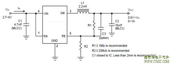
六.电路原理图
|


七,功能概述
In most applications, the CXSD62125 CXSD62125A does not dissipate much heat due to its high efficiency. But, in applications where the CXSD62125 CXSD62125A is running at high ambient tempera ture with low supply voltage and high duty cycles, the heat dissipated may exceed the maximum junction temperature of the part. If the junction temperature reaches ap-proximately 150°C, both power switches will be turned off and the SW node will become high impedance.To avoid the CXSD62125 CXSD62125A from exceeding the maximum junction temperature, the user will need to do some thermal analysis. The goal of the thermal analysis is to determine whether the power dissipated exceeds the maxi-mum junction temperature of the part. The power dissipated by the part is approximated:
PD ≅ IOUT2 x (RP-FET x D+RN-FET x (1-D))
The temperature rise is given by:
TR = (PD)(èJA)
Where PD is the power dissipated by the regulator, D is
duty cycle of main switch
D = VOUT/VIN
The èJA is the thermal resistance from the junction of the
die to the ambient temperature. The junction temperature,
TJ, is given by:
TJ = TA + TR
Where TA is the ambient temperature.
Layout Consideration
For all switching power supplies, the layout is an important step in the design; especially at high peak currents
and switching frequencies. If the layout is not carefully done, the regulator might show noise problems and duty
cycle jitter.
1. The input capacitor should be placed close to the VIN and GND. Connecting the capacitor and VIN/GND with
short and wide trace without any via holes for good input voltage filtering. The distance between VIN/GND
to capacitor less than 2mm respectively is recommended.
2. To minimize copper trace connections that can inject noise into the system, the inductor should be placed
as close as possible to the SW pin to minimize the noise coupling into other circuits.
3. The output capacitor should be place closed to converter VOUT and GND.
4. Since the feedback pin and network is a high impedance circuit the feedback network should be routed
away from the inductor. The feedback pin and feedback network should be shielded with a ground plane
or trace to minimize noise coupling into this circuit.
5. A star ground connection or ground plane minimizes ground shifts and noise is recommended.
八,相关产品 更多同类产品.......
|
Switching Regulator > Buck Converter |
|||||||||||
|
Part_No |
Package |
Architectu |
No.of PWM Outpu |
Drive Lout (A) |
Vin(V) |
Fmax Khz |
Vref (V) |
R-Top (milohm) |
R-Sync (milohm) |
Iq (No load) (uA) |
|
|
min |
max |
||||||||||
|
TQFN5x6-28 |
CM |
1 |
5 |
4.5 |
26 |
380 |
0.8 |
50 |
20 |
1000 |
|
|
SOP-8 |
CM |
1 |
2 |
4.5 |
26 |
380 |
0.8 |
100 |
1000 |
||
|
SOP-8P |
CM |
1 |
4 |
4.5 |
26 |
380 |
0.8 |
80 |
1000 |
||
|
SOT23-5|TSOT23-5 |
CM |
1 |
1 |
2.7 |
6 |
1500 |
0.6 |
280 |
250 |
25 |
|
|
SOT23-5 |
CM |
1 |
1 |
2.7 |
6 |
1500 |
0.6 |
280 |
250 |
||
|
SOP-8 |
CM |
1 |
3 |
4.3 |
14 |
500 |
0.8 |
70 |
70 |
500 |
|
|
SOP-8P |
CM |
1 |
3 |
4.3 |
14 |
500 |
0.8 |
55 |
45 |
500 |
|
|
TDFN3x3-10 |
3 |
2.6 |
5.5 |
2000 |
0.8 |
110 |
110 |
460 |
|||
|
TDFN3x3-10 |
CM |
2 |
1 |
2.7 |
6 |
1500 |
0.6 |
280 |
250 |
500 |
|
|
TDFN3x3-10 |
CM |
2 |
1 |
2.7 |
6 |
1500 |
0.6 |
280 |
250 |
||
|
TDFN2x2-6 |
CM |
1 |
1 |
2.7 |
6 |
1500 |
0.6 |
280 |
250 |
25 |
|
|
TDFN2x2-6 |
CM |
1 |
1 |
2.7 |
6 |
1500 |
0.6 |
280 |
250 |
||
|
TDFN3x3-12 |
CM |
2 |
1 |
2.7 |
6 |
1500 |
0.6 |
280 |
250 |
25 |
|
|
TDFN3x3-12 |
CM |
2 |
1 |
2.7 |
6 |
1500 |
0.6 |
280 |
250 |
||
|
TDFN 3x3 12 |
CM |
2 |
1 |
3 |
5.5 |
1500 |
0.6 |
280 |
250 |
30 |
|
|
TQFN3x3-20 |
CM |
3 |
2 |
2.9 |
5.5 |
1500 |
0.6 |
- |
- |
300 |
|
|
TDFN2x2-8 |
CM |
1 |
1 |
3.3 |
8 |
1500 |
0.6 |
280 |
250 |
25 |
|
|
SOP-8 |
CM |
1 |
2 |
4.5 |
24 |
340 |
0.925 |
110 |
110 |
1900 |
|
|
SOP-8P |
CM |
1 |
3 |
4.5 |
24 |
340 |
0.925 |
110 |
110 |
1900 |
|
|
SOP-8 |
CM |
1 |
2 |
4.5 |
24 |
340 |
0.92 |
130 |
130 |
1900 |
|
|
|
|||||||||||


发表评论