 中文
中文 English
CXSD6282A关闭和软启动功能电压型PWM控制设计欠压保护(UVP)过电流保护(OCP)
目录
1.产品概述 2.产品特点
3.应用范围 4.下载产品资料PDF文档
5.产品封装图 6.电路原理图
7.功能概述 8.相关产品
一,产品概述(General Description)
The CXSD6282 CXSD6282A is a voltage mode, synchronous PWM controller which
drives dual N-channel MOSFETs. The device integrates all of the control, monitoring and protecting functions into a single package, provides one controlled power output with under-voltage and over-current protections.The CXSD6282 CXSD6282A provides excellent regulation for output load variation. The internal 0.6V temperature-compensated reference voltage is designed to meet the requirement of low output voltage applications. The device includes a 200kHz free-running triangle-wave oscillator that is adjustable from 50kHz to 1000kHz.
The CXSD6282 CXSD6282A has been equipped with excellent protec-tion functions: POR, OCP, and UVP. The Power-On-Re-set (POR) circuit can monitor the VCC, EN, and OCSET voltage to make sure the supply voltage exceeds their threshold voltage while the controller is running. The Over-Current Protection (OCP) monitors the output cur-rent by using the voltage drop across the upper MOSFET’s RDS(ON). When the output current reaches the trip point, the controller will run the soft-start function until the fault events are removed. The Under-Voltage Protection (UVP)monitors the voltage at FB pin (V FB) for short-circuit protection. When the VFB is less than 50% of VREF, the controller will shutdown the IC directly.
二.产品特点(Features)
1.)Single 12V Power Supply Required
2.)0.6V Reference with 1% Accuracy
3.)Shutdown and Soft-Start Function
4.)1.)Programmable Frequency Range from 50 kHz to 1000kHz
5.)Voltage Mode PWM Control Design
6.)Up to 100% Duty Cycle
7.)Under-Voltage Protection (UVP)
8.)Over-Current Protection (OCP) SOP-14 Package
9.)Lead Free and Green Devices Available (RoHS Compliant)
三,应用范围 (Applications)
Graphic Cards
四.下载产品资料PDF文档
需要详细的PDF规格书请扫一扫微信联系我们,还可以获得免费样品以及技术支持!

五,产品封装图 (Package)

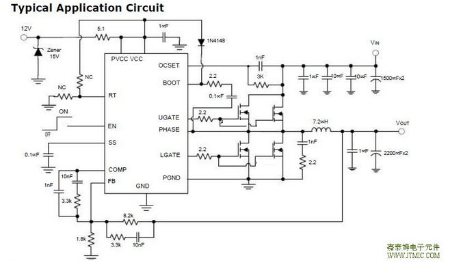
六.电路原理图

七,功能概述
Layout Consideration
In any high switching frequency converter, a correct layout is important to ensure proper operation
of the regulator.With power devices switching at 300kHz,the resulting cur-rent transient will cause
voltage spike across the i n t e r c o n n e c t i n g impedance and parasitic circuit elements. As an
example, consider the turn-off transition of the PWM MOSFET. Before turn-off, the MOSFET is
carrying the full load current. During turn-off, current stops flowing in the MOSFET and is
free-wheeling by the lower MOSFET and parasitic diode. Any parasitic inductance of the circuit
generates a large voltage spike during the switching interval. In general, using short and
wide printed circuit traces should minimize interconnect-ing impedances and the magnitude
of voltage spike.And signal and power grounds are to be kept separating till combined using
the ground plane construction or single point grounding. Figure 10 illustrates the layout,
with bold lines indicating high current paths; these traces must be short and wide. Components
along the bold lines should be placed lose together. Below is a checklist for your layout:
- Keep the switching nodes (UGATE, LGATE, and PHASE) away from sensitive small signal nodes
since these nodes are fast moving signals. Therefore,keep traces to these nodes as short as possible.
- The traces from the gate drivers to the MOSFETs (UGATE, LGATE) should be short and wide.
- Place the source of the high-side MOSFET and the drain of the low-side MOSFET as close as possible.
Minimizing the impedance with wide layout plane between the two pads reduces the voltage bounce of
the node.
- Decoupling capacitor, compensation component, the resistor dividers, boot capacitors, and SS capacitors
should be close their pins. (For example, place the decoupling ceramic capacitor near the drain of the
high-side MOSFET as close as possible. The bulk capacitors are also placed near the drain).
- The input capacitor should be near the drain of the upper MOSFET; the output capacitor should be near
the loads. The input capacitor GND should be close to the output capacitor GND and the lower MOSFET
GND.
- The drain of the MOSFETs (VIN and PHASE nodes)should be a large plane for heat sinking.
八,相关产品 更多同类产品......
|
Switching Regulator > Buck Controller |
||||||||||
|
Part_No |
Package |
Archi tectu |
Phase |
No.of PWM Output |
Output Current (A) |
Input Voltage (V) |
Reference Voltage (V) |
Bias Voltage (V) |
Quiescent Current (uA) |
|
|
min |
max |
|||||||||
|
SOP-14 QSOP-16 QFN4x4-16 |
VM |
1 |
1 |
30 |
2.9 |
13.2 |
0.9 |
12 |
8000 |
|
|
SOP-8 |
VM |
1 |
1 |
20 |
2.9 |
13.2 |
0.8 |
12 |
5000 |
|
|
SOP-8 |
VM |
1 |
1 |
20 |
2.9 |
13.2 |
0.8 |
12 |
5000 |
|
|
QFN4x4-24 |
VM |
2 |
1 |
60 |
3.1 |
13.2 |
0.6 |
12 |
5000 |
|
|
SOP-8 |
VM |
1 |
1 |
20 |
2.2 |
13.2 |
0.8 |
5~12 |
2100 |
|
|
SOP-8 |
VM |
1 |
1 |
20 |
2.2 |
13.2 |
0.8 |
5~12 |
2100 |
|
|
SOP8|TSSOP8 |
VM |
1 |
1 |
5 |
5 |
13.2 |
1.25|0.8 |
5~12 |
3000 |
|
|
SOP-8 |
VM |
1 |
1 |
10 |
3.3 |
5.5 |
0.8 |
5 |
2100 |
|
|
SOP-14 |
VM |
1 |
1 |
10 |
5 |
13.2 |
0.8 |
12 |
2000 |
|
|
TSSOP-24 |QFN5x5-32 |
VM |
1 |
2 |
20 |
5 |
13.2 |
0.6 |
5~12 |
4000 |
|
|
SOP14 QSOP16 QFN-16 |
VM |
1 |
1 |
30 |
2.9 |
13.2 |
0.9 |
12 |
4000 |
|
|
SOP-14 |
VM |
1 |
1 |
30 |
2.2 |
13.2 |
0.6 |
12 |
5000 |
|
|
SOP-14 |
VM |
1 |
1 |
30 |
2.2 |
13.2 |
0.6 |
12 |
5000 |
|
|
SOP-14 |
VM |
1 |
1 |
25 |
2.2 |
13.2 |
0.8 |
12 |
5000 |
|
|
LQFP7x7 48 TQFN7x7-48 |
VM |
1 |
6 |
0.015 |
1.4 |
6.5 |
- |
5 |
1800 |
|
|
TSSOP-24P |
VM |
1 |
2 |
20 |
2.97 |
5.5 |
0.8 |
5~12 |
5000 |
|
|
SOP-14 |
VM |
1 |
1 |
10 |
5 |
13.2 |
0.8 |
12 |
3000 |
|
|
SOP-8-P|DIP-8 |
VM |
1 |
1 |
30 |
2.9 |
13.2 |
1.2 |
12 |
3000 |
|
|
SSOP28 QFN4x4-24 |
VM |
1 |
2 |
20 |
5 |
24 |
0.9 |
5 |
1200 |
|
|
SOP-20 |
VM |
1 |
2 |
20 |
2.2 |
13.2 |
0.6 |
5~12 |
4000 |
|
|
SOP8|DFN3x3-10 |
VM |
1 |
2 |
- |
- |
- |
- |
|||


发表评论