 中文
中文 English
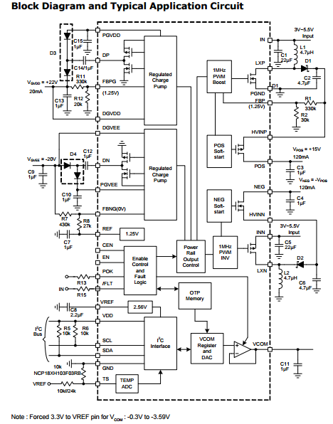
CXLC8955用于电子纸显示器的单芯片多输出PMIC两个PWM变换器分别产生正电压和负电压由两个电荷泵分别为源极驱动器和栅极驱动器提供更高的电压两个集成电源开关用于在关机模式下断开这些PWM输出与负载的连接
| 产品型号: | CXLC8955 |
| 产品类型: | 显示屏驱动 |
| 产品系列: | 液晶显示驱动 |
| 产品状态: | 量产 |
| 浏览次数: | 939 次 |
产品简介
技术参数
| 输入电压范围 (VIN) | - 3~5.5V |
|---|---|
| 输出电压 (VOUT) | ADJ |
| 输出电流 (IOUT) | 1.8A |
| 工作频率 | 1000Khz |
| 转换效率 | 95% |
| 封装类型 | TQFN5x5-32 |
| Iq | 2000 |
| Features | Vref(V)1.25 |
| Pf value | .9 |
| Topology | 液晶显示驱动 |
| Interface | Two set for VGH,VGL |
| Led count | 4*32 |
| Protection | OVP/OCP/短路保护 |
| Topology type | Boost Charge pump |
| Dimming method | PSM/PWM |
| Application type | 显示屏驱动 |
产品详细介绍
目录
7.相关产品
产品概述 返回TOP
The CXLC8955 is a single chip, multi outputs PMIC for Epaper displays. Two PWM converters respectively generate positive and negative voltages which are boosted to higher voltage by two charge pumps for both source and gate drivers. Two integrated power switches are used to disconnect these PWM outputs from load in shutdown mode. All PWM and charge pump output voltages are adjustable by external resistors and their power on/off timings can be individually programmable via I2C interface. One accurate VCOM voltage, for backplane biasing, is adjustable via I2C interface from -0.3V to -2.85V with 10mV per step. The VCOM is capable of sourcing and sinking current, depending on panel condition, at lease 100mA. An external negative temperature coefficient(NTC) resistor is incorporated to sense remote temperature. This remote temperature sensing can be used to monitor the battery’s surface temperature to avoid over heating. The temperature data is mapped from the voltage on TS pin according to a preset conversion table. Approximately every 250ms the CXLC8955 executes the voltage/temperature conversion and stores the temperature date in register in two’s complement format. The CXLC8955 is available in a space saving TQFN5x5 32-pin package and is specified over the -40oC to +85oC extended temperature range.
产品特点 返回TOP
· Single Chip Power Management Solution for Epaper Displays
· Input SupplyVoltage Range: 3.0~5.5V
· I 2C Series Interface
· Boost Converter for Positive Rail Base (HVINP)
· Inverting Buck-Boost Converter for Negative Rail Base (HVINN)
· Accurate Voltage Tracking between HVINP and HVINN: +50mV
· Integrated Two Power Switches with Soft-start Control for Source Driver Supply -POS: +15V/120mA -NEG: -15V/120mA
· Two Charge Pump for Gate Driver Supply
-DGVDD: +22V/20mA
-DGVEE:-22V/20mA
· Accurate and Adjustable VCOM Voltage for Panel Backplane Biasing
- -0.3 to -2.85V/100mA, 10mV per step
-8-bit Control
· Programmable Turn-on/Turn-off Timing in every Output Voltage
· Remote Temperature Sensing
· POK Output
· FAULTOutput
· Enable Input
· Current Limit Protection
· Over Temperature Protection
· Fault Events Report in Every Output for Easy Debugging
· 1MHz Fixed PWM Frequency
· Up to 85% efficiency for the Boost
· Internal Soft Start Control
· Available in TQFN5x5-32 Package
· Halogen and Lead Free Available (RoHS Compliant)
应用范围 返回TOP
· E-paper Display
技术规格书(产品PDF) 返回TOP
需要详细的PDF规格书请扫一扫微信联系我们,还可以获得免费样品以及技术支持!

产品封装图 返回TOP


电路原理图 返回TOP


相关芯片选择指南 返回TOP 更多同类产品.......
|
PMIC > LCD Bias Converter |
|||||||||||||||
|
Part_No |
Package |
Topology |
Buffer for Vcom |
Switch Current Limit (A) |
Vin (V) |
Fmax Khz |
SYNC ASYNC |
PFM/PSM |
Vref (V) |
R-Top milohm |
Iq(No load) (uA) |
En pin |
POK |
Charge Pump Output |
|
|
min |
max |
||||||||||||||
|
TQFN3 x3-20 |
Boos tCharge pump |
Yes |
2 |
2.7 |
5.5 |
1500 |
ASYNC |
PSM/PWM |
1.25 |
500 |
300 |
Yes |
No |
Two set for VGH, VGL |
|
|
TQFN3 x3-20 |
Boos tCharge pump |
2 |
2.9 |
5.5 |
1000 |
ASYNC |
PSM/PWM |
1.25 |
Yes |
No |
Two set for VGH,VGL |
||||
|
TQFN5 x5-32 |
Boost Charge pump |
Yes |
1.8 |
3 |
5.5 |
1000 |
ASYNC |
PSM/PWM |
1.25 |
250 |
2000 |
Yes |
No |
Two set for VGH,VGL |
|
|
WLCSP1.92 x1.28-15 |
Boost Charge pum |
0.6 |
2.5 |
5.5 |
1800 |
SYNC |
PSM/PWM |
540 |
Yes |
No |
Two set for VGH,VGL |
||||

用户评论