CXSU63133一种紧凑型、PFM模式和升级型具有低静态电流的DC-DC转换器。国际米兰-
nal同步整流器降低了成本和PCB空间不需要外部肖特基二极管。内部开关的低导通电阻提高了
效率高达92%。启动电压有保证低于1V
-
[ 产品资料下载 ]
目录
1.产品概述 2.产品特点
3.应用范围 4.下载产品资料PDF文档
5.产品封装图 6.电路原理图
7.功能概述 8.相关产品
一,产品概述(General Description)
The CXSU63133 is a compact, PFM mode, and step-up
DC-DC converter with low quiescent current. The inter-
nal synchronous rectifier reduces cost and PCB space
by eliminating the need for an external Schottky diode.
Low on-resistance of the internal switches improves the
efficiency up to 92%. The start-up voltage is guaranteed
below 1V. After start-up, the device can operate with input
voltage down to 0.7V. The CXSU63133 is suitable for por-
table battery-powered applications. Consuming only 11μA
quiescent current and an optimized control scheme al-
lows the device to operate at very high efficiency over the
entire load current range.
二.产品特点(Features)
1.)0.9V Typical Start-up Input Voltage
2.)11μA Typical No Load Quiescent Current
3.)PFM Operation
4.)High Efficiency up to 92%
5.)Fixed 1.8V, 2.6V, 2.8V, 3V, 3.3V, 3.8V, 4.5V or 5V
6.)Output Voltage
7.)600mA Internal Switch Current
8.)Internal Synchronous Rectifier
9.)SOT-89 Package
10.)Lead Free and Green Devices Available
(RoHS Compliant)
三,应用范围 (Applications)
Toy
Wireless Mouse
Portable Instrument
四.下载产品资料PDF文档
需要详细的PDF规格书请扫一扫微信联系我们,还可以获得免费样品以及技术支持!

五,产品封装图 (Package)
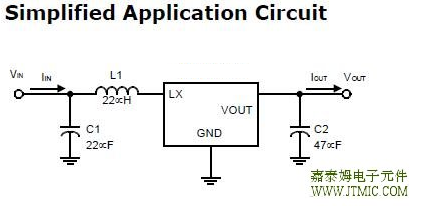
六.电路原理图
七,功能概述
Inductor Selection
The inductor value determines the inductor ripple current
and affects the load transient response. It is recom-
mended to select the boost inductor in order to keep the
maximum peak inductor current below the current limit
threshold of the power switch. For example, the current
limit threshold of the CXSU63133’s switch is 600mA. For
choosing an inductor which has peak current passed,
firstly, it is necessary to consider the output load (IOUT),
input (VIN), and output voltage (VOUT). Secondly, the de-
sired current ripple in the inductor also needed to be
taken into account. The current was calculated in “Output
Capacitor Selection”. Since the output ripple is the prod-
uct of the peak inductor current and the output capacitor
ESR, the larger inductor value reduces the inductor cur-
rent ripple and output voltage ripple but typically offers a
larger physical size.
|
PIN |
FUNCTION |
|
|
NO. |
NAME |
|
|
1 |
LX |
Junction of N-FET and P-FET Drains. Connect the inductor here and minimize the trace area for |
|
2 |
VOUT |
Converter output and control circuitry bias supply pin. |
|
3 |
GND |
Ground. |
Control Scheme
The converter monitors the output voltage. When the in-
ternal feedback voltage falls below the reference voltage,
the main switch turns on and the inductor current ramps
up. The main switch turns off when the current reaches
the peak current limit of typical 600mA. The second crite-
rion that turns off the switch is the maximum on-time of
4μs (typical). As the main switch is turned off, the syn-
chronous switch is turned on and delivers the current to
the output. The main switch remains off for a minimum of
900ns (typical), or until the internal feedback voltage drops
below the reference voltage. By the control scheme with
low quiescent current of 11μA (typical), the converter gets
high efficiency over a wide load range.
Start-Up
A startup oscillator circuit is integrated in the CXSU63133.
When the power is applied to the device, the circuit pumps
the output voltage high. Once the output voltage reaches
1.4V (typ), the main DC-DC circuitry turns on and boosts
the output voltage to the final regulation point.
Synchronous Rectification
The internal synchronous rectifier eliminates the need
for an external Schottky diode, thus, reducing cost and
board space. During the cycle off-time, the P-channel
MOSFET turns on and shunts the MOSFET body diode.
As a result, the synchronous rectifier significantly improves
efficiency without the addition of an external component.
Conversion efficiency can be as high as 92%.
Over-Temperature Protection
The over-temperature circuit limits the junction tempera-
ture of the CXSU63133. When the junction temperature ex-
ceeds 150°C, a thermal sensor turns off the power
MOSFETs, allowing the devices to cool. The thermal sen-
sor allows the converter to start a start-up process and
regulate the output voltage again after the junction tem-
perature cools by 40°C. The OTP is designed with a 40°C
hysteresis to lower the average TJ during continuous ther-
mal overload conditions, increasing lifetime of the device.
八,相关产品 更多同类产品......
|
Switching Regulator > Boost Converter |
|||||||||||
|
Part_No |
Package |
Archi-tecture |
Input Voltage |
Max Adj. Output Voltage |
Switch Current Limit (max) |
Fixed Output Voltage |
Switching Frequency |
Internal Power Switch |
Sync. Rectifier |
||
|
min |
max |
min |
max |
(A) |
(V) |
(kHz) |
|||||
|
SOT89 |
VM |
0.9 |
5.5 |
2.5 |
5.5 |
0.5 |
1.8|2.6|2.8|3 |3.3|3.8|4.5|5 |
- |
No |
Yes |
|
|
MSOP8|TSSOP8 |SOP8 |
VM |
2.5 |
5.5 |
2.5 |
- |
- |
- |
200 ~ 1000 |
No |
No |
|
|
TSSOP8|SOP-8P |
VM |
1 |
5.5 |
2.5 |
5 |
1 |
2.5|3.3 |
300 |
Yes |
Yes |
|
|
SOP8 |
CM |
3 |
40 |
1.25 |
40 |
1.5 |
- |
33 ~ 100 |
Yes |
No |
|
|
TQFN5x5-32 |
CM |
2.5 |
6.5 |
2.5 |
18 |
3 |
No |
1200 |
Yes |
No |
|
|
TSOT23-5 TDFN2x2-6 |
CM |
2.5 |
6 |
2.5 |
20 |
2 |
- |
1500 |
Yes |
No |
|
|
TQFN4x4-6 TDFN3x3-12 |
CM |
1.8 |
5.5 |
2.7 |
5.5 |
5 |
- |
1.2 |
Yes |
Yes |
|
|
SOT23-5 |
CM |
2.5 |
6 |
2.5 |
32 |
1 |
- |
1000 |
Yes |
No |
|
|
TSOT-23-6 TDFN2x2-8 |
CM |
1.2 |
5.5 |
1.8 |
5.5 |
1.2 |
- |
1.2 |
Yes |
Yes |
|
◀ 上一篇:同步PFM开关型DC/DC升压转换器CXSU63132振荡频率为300KHz电力供应音频设备输出电压为2.0V~5.0V
下一篇▶:2.5至5.5V输入电压CXSU63134单脉冲宽度调制升压DC-DC控制器软启动和短路检测功能振荡器开关频率
| 热门信息 |
|---|
| 最新信息 |
|---|
| 推荐信息 |
|---|