|
CXSD6285双PWM降压控制器和一个内部线性调节器用于DDR存储器和MCH电源解决方案两个同步PWM buck控制ler驱动四个N通道mosfet | |||||||||||||||||||||||||||||||||||||||||||||||||||||||||||||||||||||||||||||||||||||||||||||||||||||||||||||||||||||||||||||||||||||||||||||||||||||||||||||||||||||||||||||||||||||||||||||||||||||||||||||||
|
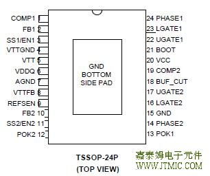
目录 1.产品概述 2.产品特点 一,产品概述(General Description) The CXSD6285 integrates Dual PWM buck controllers and an internal linear regulator for DDR memory and MCH power solution. The two synchronous PWM buck control-lers drive four N-channel MOSFETs for DDR memory sup-ply voltage (VDDQ) and MCH regulator. The internal regu-lator is designed to track at the half of the reference volt-age with sourcing and sinking current for DDR memory termination regulator (VTT). 1.)Provide Synchronous Rectified Buck PWM Controllers for VDDQ and VMCH DDR Memory and MCH Power Supply 需要详细的PDF规格书请扫一扫微信联系我们,还可以获得免费样品以及技术支持! 五,产品封装图 (Package)
六.电路原理图
七,功能概述 Output Inductor Selection 八,相关产品 更多同类产品......
发表评论
| |||||||||||||||||||||||||||||||||||||||||||||||||||||||||||||||||||||||||||||||||||||||||||||||||||||||||||||||||||||||||||||||||||||||||||||||||||||||||||||||||||||||||||||||||||||||||||||||||||||||||||||||
发表时间:2020-04-22浏览次数:160


| 最新信息 |
|---|
| 热门信息 |
|---|
| 推荐信息 |
|---|
| 头条信息 |
|---|